Module IC package structure and method for making the same

Inactive Publication Date: 2012-06-07
ANHUI HAIHUA CHEM
View PDF1 Cites 13 Cited by
  • Summary
  • Abstract
  • Description
  • Claims
  • Application Information

AI Technical Summary

Benefits of technology

[0012]Therefore, the metal shielding layer on the package resin body can electrically contact the grounding pad of the circuit substrate through the at least one elastic conductive element, thus the instant disclosure can generate the electrical shield function to prevent the electronic elements from being interfered by external environment.

Problems solved by technology

However, while the functions of the devices can be increased by integrating a lot of functional modules, the design of a multiple function device with small dimensions is still difficult.
However, up to the present the production of the shielding structures adds disproportional costs and time expenditure to the total manufacturing costs.
In many cases the shielding structure is realized as a sheet steel casing around the wireless device or circuit module, necessitating the manufacture of costly dies for each shielding structure shape.
In this case each shape to be cast requires the manufacture of a specific casting mold which involves manual work, leading to high costs.
Furthermore, the assembly of the metal casings and the circuit modules is usually performed manually thus further increases costs.

Method used


Image

  • Module IC package structure and method for making the same
  • Module IC package structure and method for making the same
  • Module IC package structure and method for making the same

Examples


first embodiment

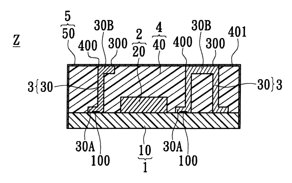
[0029]Referring to FIGS. 1 and 1A to 1H, the instant disclosure provides a method for making a module IC package structure Z with electrical shield function, comprising the steps of:

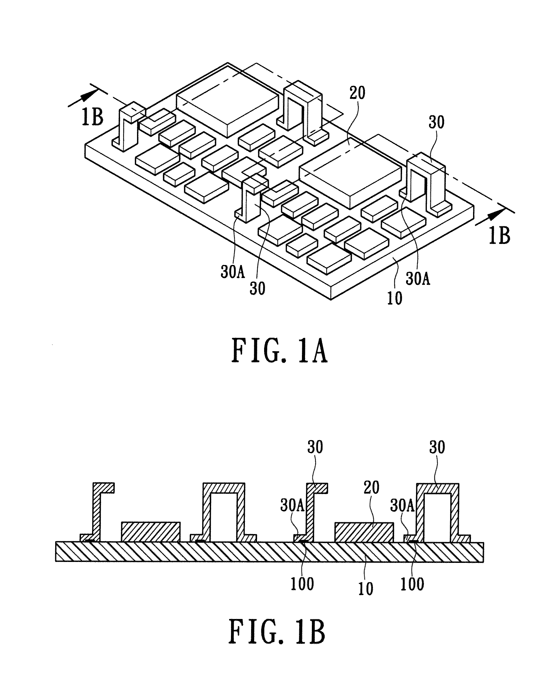
[0030]The step S100 is that: referring to FIGS. 1, 1A and 1B, providing at least one circuit substrate 10 having at least four grounding pads 100. For example, a predetermined pattern (not shown) and four or more than four grounding pads 100 can be formed on the top surface of the circuit substrate 10 in advance.

[0031]The step S102 is that: referring to FIGS. 1, 1A and 1B, placing a plurality of electronic elements 20 on the circuit substrate 10 to electrically connect to the circuit substrate 10. For example, each electronic element 20 may be a resistance, a capacitance, an inductance, a function chip having a predetermined function or a semiconductor chip having a predetermined function etc. Thus, any type of electronic component can be applied to the instant disclosure.

[0032]The step S104 is that: ref...

second embodiment

[0038]Referring to FIGS. 2A and 2B, the instant disclosure provides a method for making a module IC package structure Z with electrical shield function, comprising the steps of:

[0039]The step S200 is that: referring to FIGS. 2A and 2B(A), providing at least one circuit substrate 10 having at least four grounding pads 100.

[0040]The step S202 is that: referring to FIGS. 2A and 2B(A), placing a plurality of electronic elements 20 on the circuit substrate 10 to electrically connect to the circuit substrate 10.

[0041]The step S204 is that: referring to FIGS. 2A and 2B(A), placing at least four elastic conductive elements 30 on the circuit substrate 10, wherein each elastic conductive element 30 has a first end portion 30A electrically connected to each grounding pad 100 and a second end portion 30B.

[0042]The step S206 is that: referring to FIGS. 2A and 2B(A), forming a package resin body 40 on the circuit substrate 10 to cover the electronic elements 20 and one part of each elastic conduc...

third embodiment

[0048]Referring to FIGS. 3A and 3B, the instant disclosure provides a method for making a module IC package structure Z with electrical shield function, comprising the steps of:

[0049]The step S300 is that: referring to FIGS. 3A and 3B(A), providing at least one circuit substrate 10 having at least four grounding pads 100.

[0050]The step S302 is that: referring to FIGS. 3A and 3B(A), placing a plurality of electronic elements 20 on the circuit substrate10 to electrically connect to the circuit substrate 10.

[0051]The step S304 is that: referring to FIGS. 3A and 3B(A), placing at least four elastic conductive elements 30 on the circuit substrate 10, wherein each elastic conductive element 30 has a first end portion 30A electrically connected to each grounding pad 100 and a second end portion 30B.

[0052]The step S306 is that: referring to FIGS. 3A and 3B(A), forming a package resin body 40 on the circuit substrate 10 to cover the electronic elements 20 and each elastic conductive element ...


PUM


Abstract

A module IC package structure includes a substrate unit, an electronic unit, a conductive unit, a package unit and a shielding unit. The substrate unit includes a circuit substrate having at least one grounding pad. The electronic unit includes a plurality of electronic elements electrically connected to the circuit substrate. The conductive unit includes at least one elastic conductive element disposed on the circuit substrate, and the elastic conductive element has a first end portion electrically connected to the grounding pad. The package unit includes a package resin body disposed on the circuit substrate to cover the electronic elements and one part of the elastic conductive element, and the elastic conductive element has a second end portion is exposed from the package resin body. The shielding unit includes a metal shielding layer formed on the outer surface of the package resin body to electrically contact the second end portion.

Description

BACKGROUND OF THE INVENTION[0001]1. Field of the Invention[0002]The instant disclosure relates to a module IC (integrated circuit) package structure and a method for making the same, and more particularly, to a module IC package structure with electrical shield function and a method for making the same.[0003]2. Description of Related Art[0004]As integrated circuit technology has been rapidly developing, a variety of devices using the technology are developed continuously. Because the functions of the devices are rapidly added, most devices are implemented in a modular way. However, while the functions of the devices can be increased by integrating a lot of functional modules, the design of a multiple function device with small dimensions is still difficult.[0005]In the semiconductor manufacturing process, a high level technology is used to manufacture a small chip or component. Therefore, the module manufacturer can design a functional module with small dimensions, and the device ca...

Claims


Application Information

Patent Timeline
IPC IPC(8): H01L23/552H01L21/50
CPCH01L21/561H01L2924/01033H01L23/49811H01L23/552H01L24/97H01L2924/01082H01L2924/19041H01L2924/19042H01L2924/19043H01L2924/19105H01L2924/19107H01L2924/01087H01L2924/01005H01L2924/01006H01L23/3121H01L2924/14H01L2924/00
Inventor HUANG, CHUNG-ERKUO, MING-TAI
Owner ANHUI HAIHUA CHEM
Why Eureka
Try Eureka