Aligned nanoarray and method for fabricating the same

Inactive Publication Date: 2012-06-14
TRACENSE SYST
View PDF4 Cites 10 Cited by
  • Summary
  • Abstract
  • Description
  • Claims
  • Application Information

AI Technical Summary

Benefits of technology

[0034]Unless otherwise defined, all technical and/or scientific terms used herein have the same meaning as commonly understood by one of ordinary skill in the art to which the invention pertains. Although methods and materials similar or equivalent to those described herein can be used in the practice

Problems solved by technology

A major impediment to the emergence of this new generation is the ability to effectively grow and harvest nanowires and other nanostructures that have consistent characteristics.
Large-scale assembly of nanowire and nanotube elements presents a significant challenge facing their integration in electronic applications.

Method used


Image

  • Aligned nanoarray and method for fabricating the same
  • Aligned nanoarray and method for fabricating the same
  • Aligned nanoarray and method for fabricating the same

Examples


examples

[0125]Reference is now made to the following examples, which together with the above descriptions illustrate some embodiments of the invention in a non limiting fashion.

[0126]Prototype nanostructure arrays and circuit boards have been manufactured according to the teachings of some embodiments of the present invention.

Materials and Methods

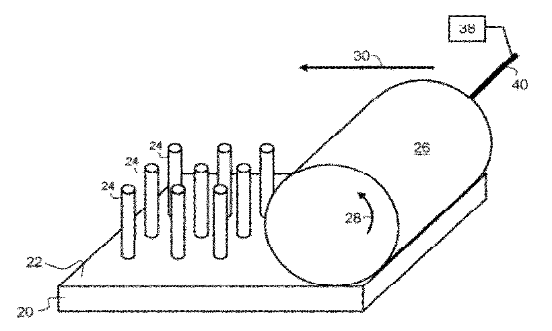
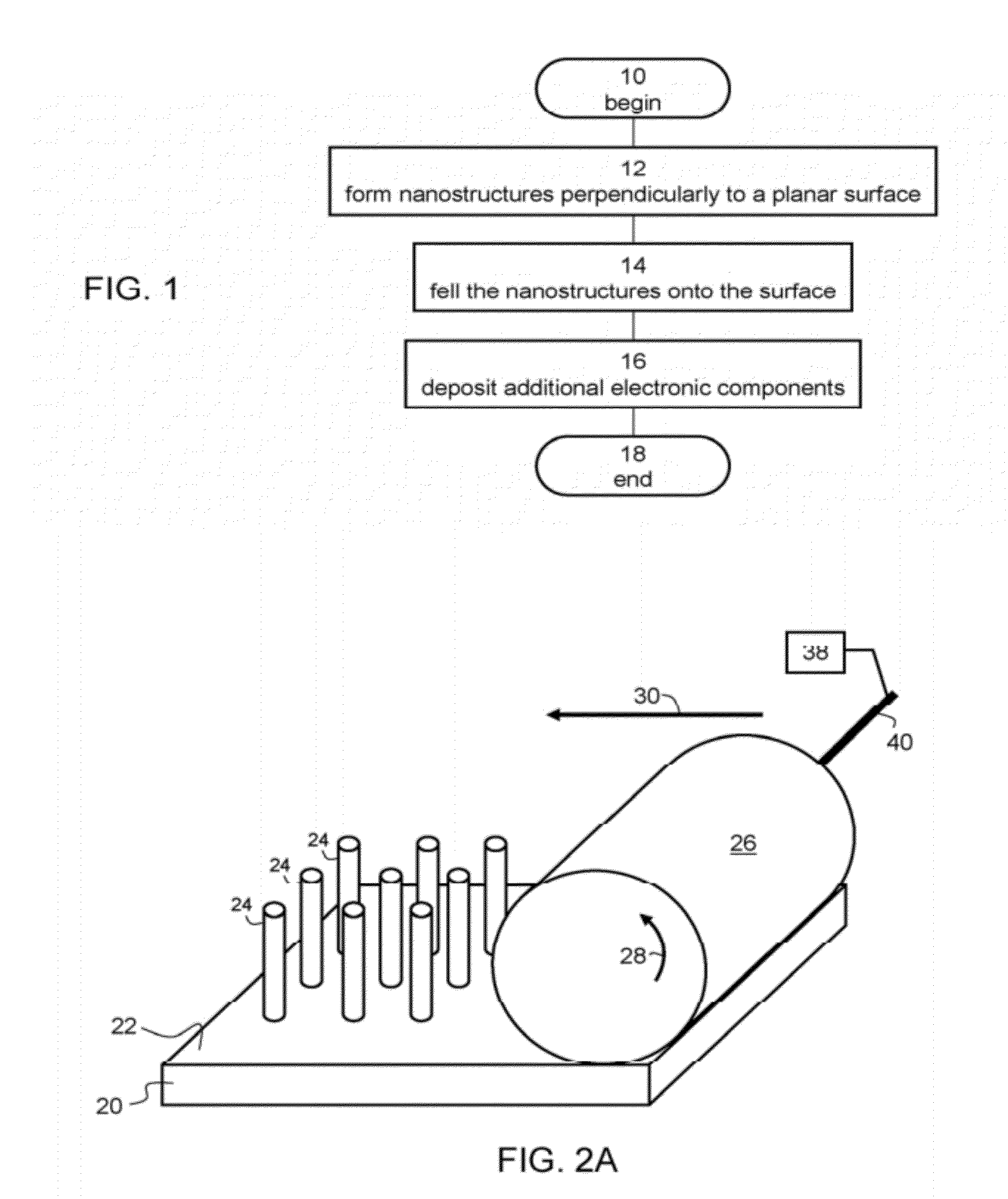
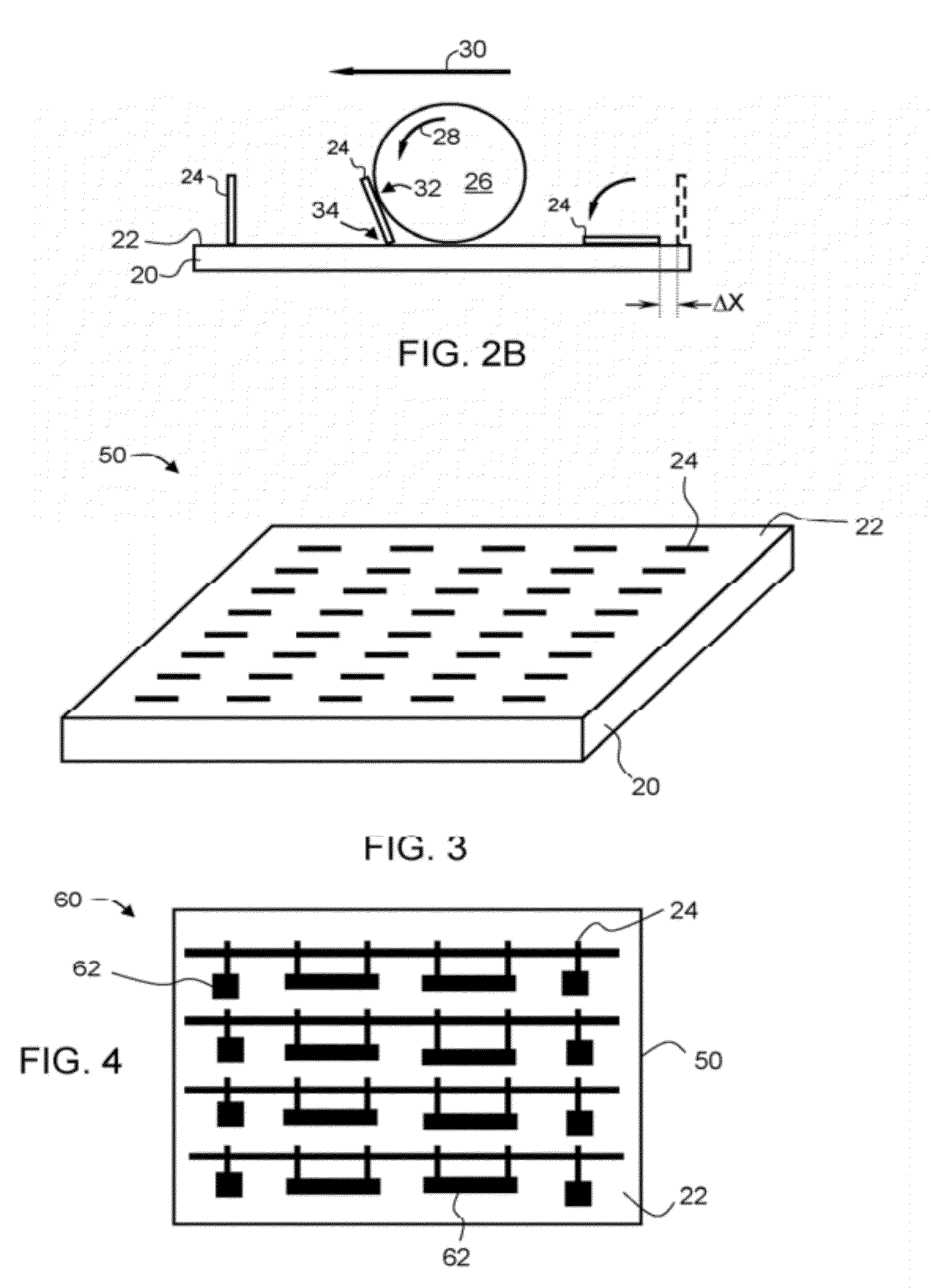
[0127]The procedure is depicted in FIGS. 6A-D. Metal nanoisland arrays were created on a planar surface (FIG. 6A). Subsequently, nanowire arrays were formed gridwise by a destructive or constructive technique at the locations of the array (FIG. 6B). The nanowires were then felled using a roller device (FIG. 6C) to form an array of nanowires (FIG. 6D) aligned generally parallel to the surface and generally parallel to each other, at approximately the locations of the islands. Additional electronic components, specifically source-drain electrodes and contacts were subsequently deposited on the array.

Fabrication of Nanoisland Arrays

[0128]Si wafers wer...


PUM

PropertyMeasurementUnit
Lengthaaaaaaaaaa
Fractionaaaaaaaaaa
Angleaaaaaaaaaa

Abstract

An elongated nanostructure is formed on a planar surface of a substrate such that the nanostructure is oriented generally perpendicularly to the surface. The nanostructure is then felled onto the surface such that it is oriented generally parallel to the surface.

Description

FIELD AND BACKGROUND OF THE INVENTION[0001]The present invention, in some embodiments thereof, relates to nanofabrication and, more particularly, but not exclusively, to an aligned nanoarray and method for fabricating an aligned nanoarray.[0002]As the market for low-cost and / or high-performance / density micron- and nano-scale electronic and electromechanical integrated circuits increases, many new assembly techniques investigated and commercialized. At the same time, there has also been a continued interest in scaling to nanometer dimensions the size of individual devices within such integrated circuits. In this respect, nanostructures, and in particular elongated nanostructures such as nanowires and nanotubes, have the potential to facilitate a whole new generation of electronic devices. The small dimensions of electrically-conducting nanowires such as carbon nanotubes make them useful as nano-scale, vertically-connecting wires between circuit device layers as well as in-plane conne...

Claims


Application Information

Patent Timeline
IPC IPC(8): B32B3/00B05C11/02H05K3/02B05D1/12B82Y30/00
CPCB82Y10/00B82Y30/00B82Y40/00Y10T428/24355H01L29/0665H01L29/0673Y10T29/49155H01L21/67092
Inventor PATOLSKY, FERNANDODUCOBNI, TAMIRPEVZNER, ALEXANDERENGEL, YONIELNATHAN, ROEYBEN-ISHAI, MOSHIT
Owner TRACENSE SYST
Why Eureka
Try Eureka