
Display substrate, method of manufacturing the same, and display panel having the same

a technology of display substrate and manufacturing method, which is applied in the manufacture of electric discharge tubes/lamps, basic electric elements, instruments, etc., can solve the problems of longening the manufacturing time and cost of display substrate, and achieve the effect of simplifying the manufacturing process

Active Publication Date: 2012-06-21
SHENZHEN CHINA STAR OPTOELECTRONICS TECH CO LTD
View PDF5 Cites 15 Cited by
  • Summary
  • Abstract
  • Description
  • Claims
  • Application Information

AI Technical Summary

Benefits of technology

[0009]Exemplary embodiments of the present invention provide a display substrate which is flatter or more planar, having a reduced step difference in elevations of an exposed surface thereof
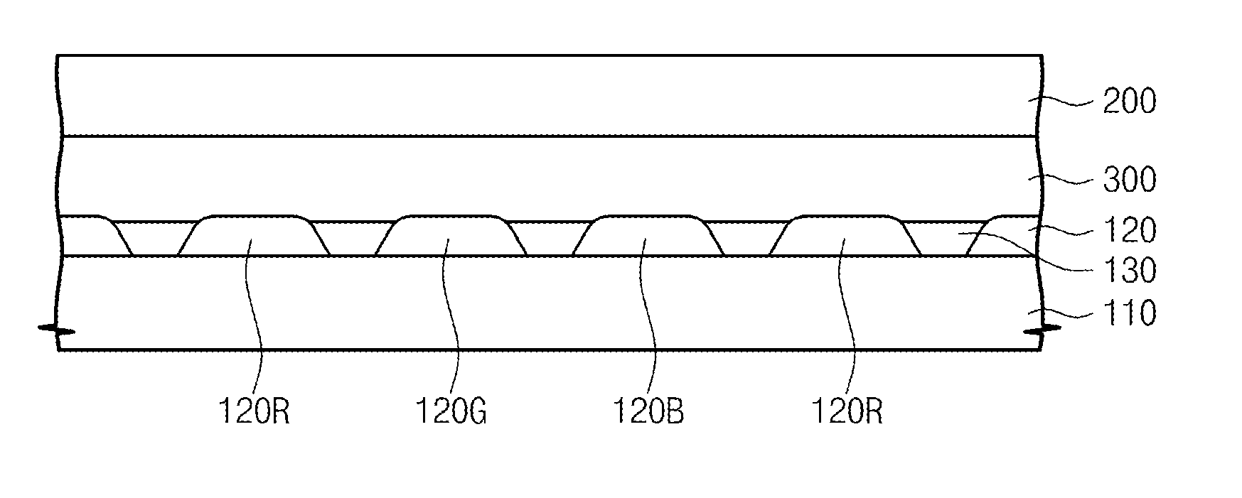
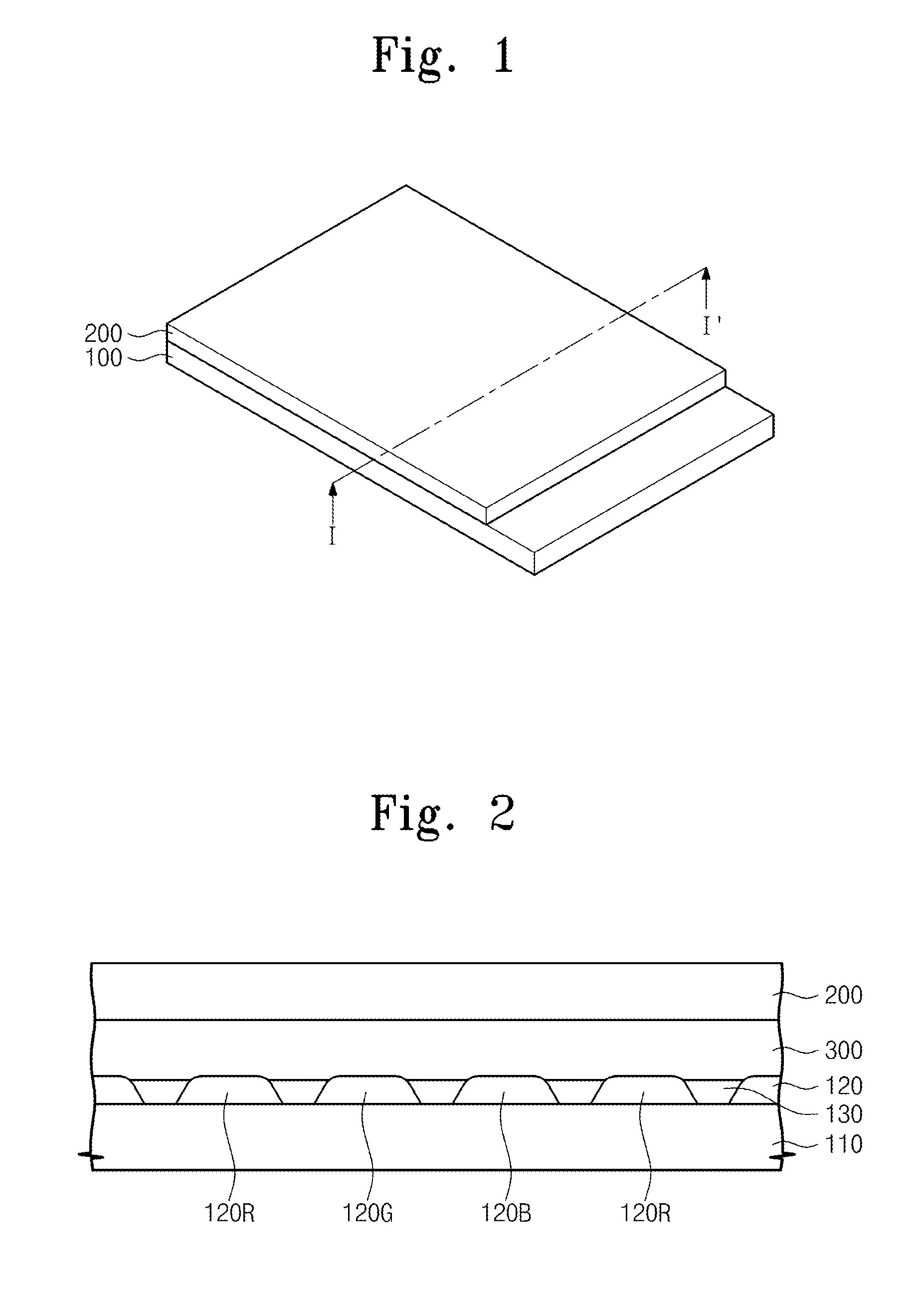
[0026]As described above, the edge portion of the color filter overlaps with the tapered edge portion of the light blocking layer, so that step differences in height between the two may be reduced and the display substrate may have a substantially flat surface even if an overcoat layer is not provided.
[0027]In addition, the display substrate can be manufactured without performing an exposure process, so that the manufacturing process can be simplified.

Problems solved by technology

However, the photolithography process typically requires coating, exposure, development and curing processes, lengthening the manufacturing time for the display substrate, as well as its cost.

Method used


Image

  • Display substrate, method of manufacturing the same, and display panel having the same
  • Display substrate, method of manufacturing the same, and display panel having the same
  • Display substrate, method of manufacturing the same, and display panel having the same

Examples


Embodiment Construction

[0037]The present invention can be modified in various forms and may not be limited to the following embodiments but include various applications and modifications. The following embodiments are provided to clarify the technical spirit disclosed in the present invention and to sufficiently transmit the technical spirit of the present invention to the one having mean knowledge and skill in this field. Therefore, the scope of the present invention should not be limited to the following embodiments.

[0038]When describing each attached drawing, similar reference numerals are designated as similar components. In addition, the size of the layers and regions of the attached drawings along with the following embodiments are simplified or exaggerated for precise explanation or emphasis and the same reference numeral represents the same component. The terms ‘first’ and ‘second’ are used for the purpose of explanation about various components, and the components are not limited to the terms ‘fi...


PUM


Abstract

A display panel includes a base substrate having a plurality of pixel areas, in which each pixel area includes a plurality of sub-pixel areas, a light blocking layer pattern generally defining the sub-pixel areas, and a plurality of color filter patterns. Upper surfaces of the light blocking layer pattern and the plurality of color filter patterns collectively form a generally flat surface.

Description

CROSS-REFERENCE TO RELATED APPLICATION[0001]This application relies for priority upon Korean Patent Application No. 10-2010-0131735 filed on Dec. 21, 2010, the contents of which are herein incorporated by reference in their entirety.BACKGROUND[0002]1. Field of Disclosure[0003]Embodiments of the present invention relate generally to flat panel displays. More particularly, embodiments of the present invention relate to a display substrate having a reduced step difference on an exposed surface thereof, a method of manufacturing the display substrate, and a display panel having the display substrate.[0004]2. Description of the Related Art[0005]A display panel of a flat-panel display substrate typically includes a plurality of pixels to display colors. A pixel area is generally defined by a light blocking layer, and a plurality of color filters is provided in the pixel area.[0006]Recently, as pixel sizes have shrunk, increasing use has been made of a photosensitive organic material that ...

Claims


Application Information

Patent Timeline
IPC IPC(8): G02F1/1335H01J9/24
CPCG02B5/003G02F1/133514G02F1/133512G02B5/201
Inventor KANG, HOONKIM, JAE-SUNGCHOI, JIN-YOUNGCHO, YOUNGJEJEON, WOO-SEOK
Owner SHENZHEN CHINA STAR OPTOELECTRONICS TECH CO LTD
Learn More