

Transparent Electrode and Organic Light Emitting Diode Device Including the Transparent Electrode and Method of Manufacturing the Same
a technology of light-emitting diodes and transparent electrodes, which is applied in the direction of transistors, semiconductor lamps, basic electric elements, etc., can solve problems such as display defects, and achieve the effect of preventing display defects
Active Publication Date: 2012-07-05
SAMSUNG DISPLAY CO LTD
View PDF9 Cites 41 Cited by
- Summary
- Abstract
- Description
- Claims
- Application Information
AI Technical Summary
Benefits of technology
[0009]An exemplary aspect of the present invention provides a transparent electrode that prevents display defects.
[0031]Accordingly, the transparent electrode made of a conductive oxide may have no pin hole and thus, prevent display defects.
Problems solved by technology
The pin hole may play a role of being a passage for a chemical solution such as an etchant and the like flown inside the transparent electrode during the subsequent process, resulting in display defects.
Method used
View moreImage
Smart ImageViewing Examples

Examples
example
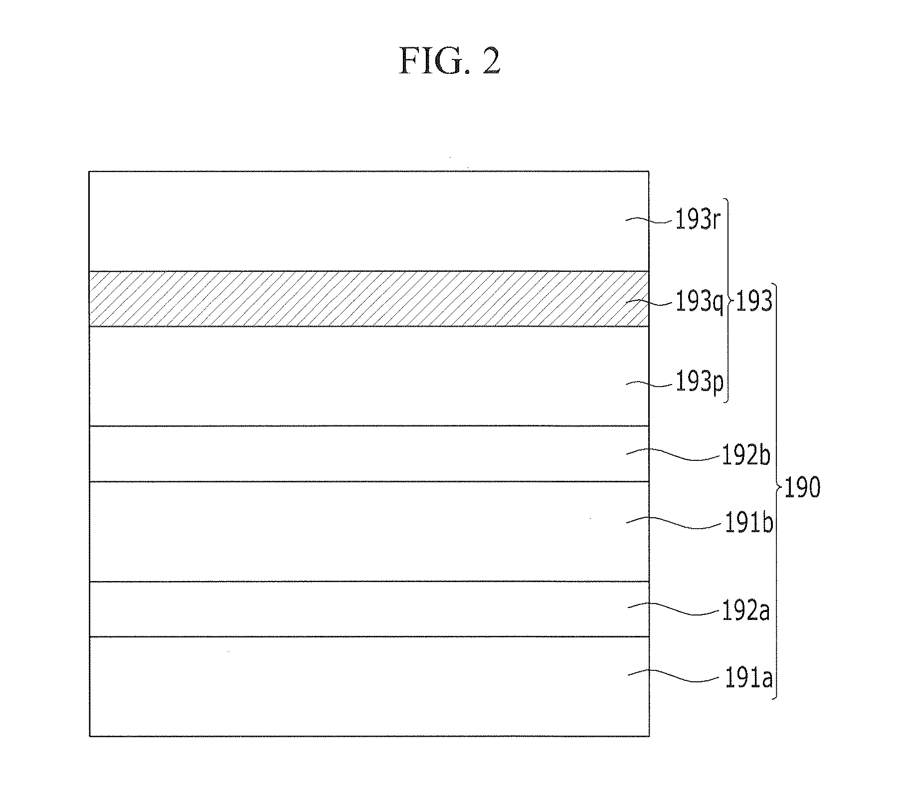
[0121]Fabricated was a thin film transistor according to the aforementioned embodiment. Then, a pixel electrode was formed thereon by respectively laminating ITO / Ag / ITO / Ni / ITO to respectively have a thickness or a concentration of 70 Å, 150 Å, 150 Å, 1×10¹⁵ atoms / cm2, and 150 Å, respectively and then, patterned using a nitric acid-based etching solution to fabricate a transparent electrode.
Login to View More PUM
| Property | Measurement | Unit |
|---|---|---|
| light-transmission | aaaaa | aaaaa |
| conductive | aaaaa | aaaaa |
| releases energy | aaaaa | aaaaa |
Abstract
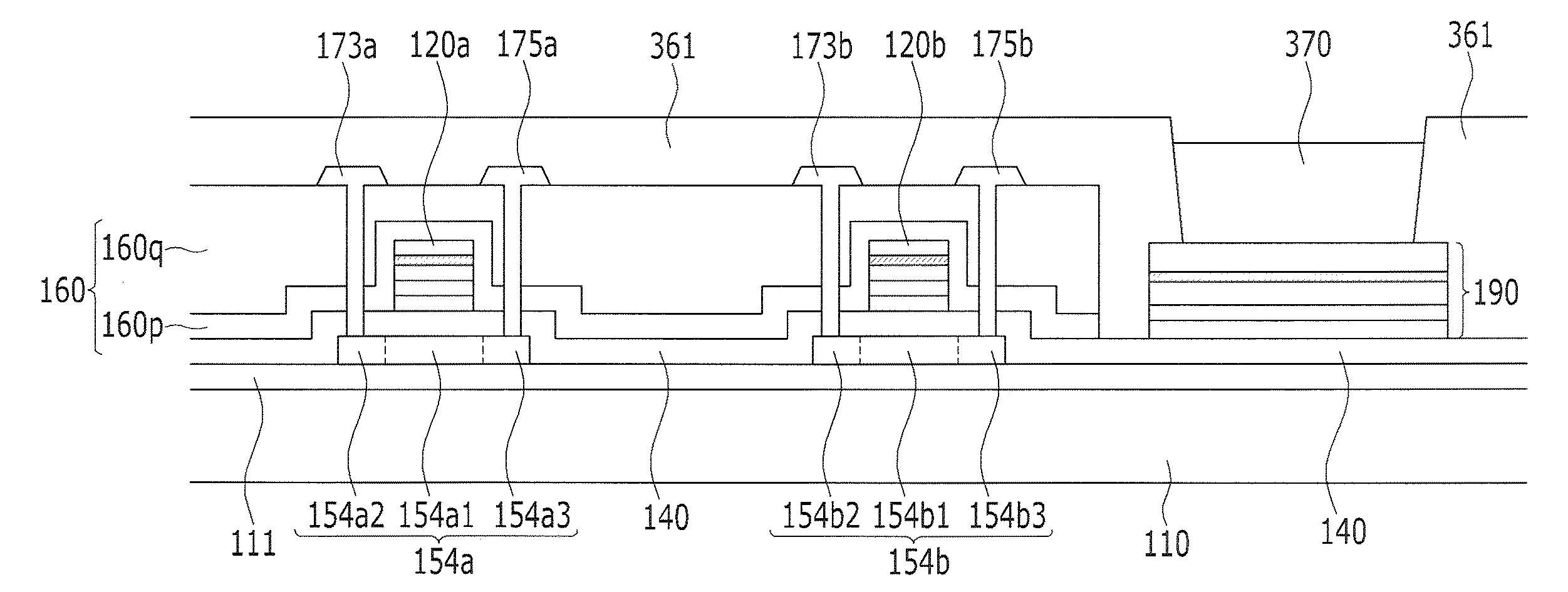
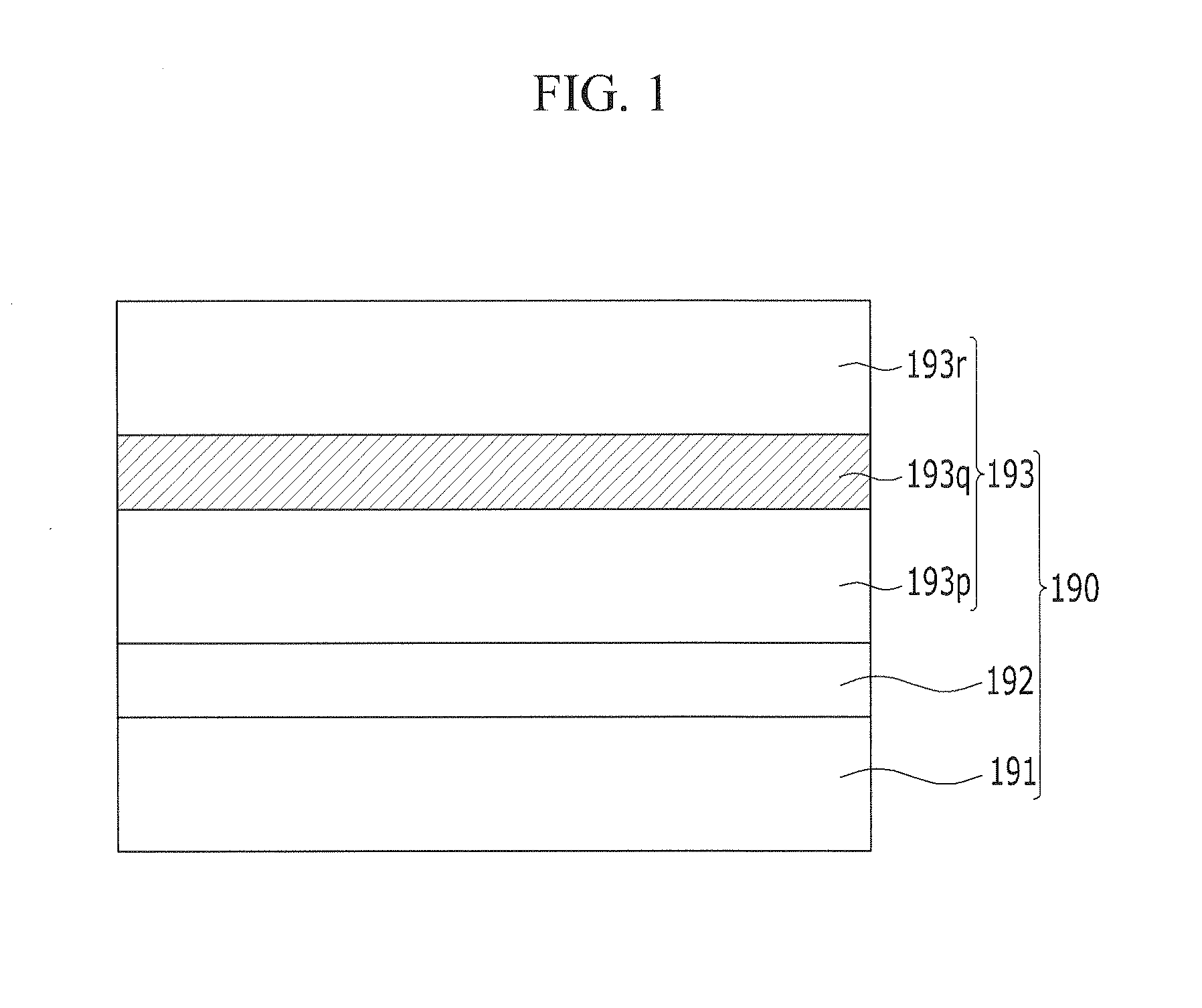
Disclosed are a transparent electrode including a first light-transmission layer, a metal layer, and a second light-transmission layer sequentially formed, an organic light emitting device including the transparent electrode, and a method of manufacturing the same. The second light-transmission layer includes a conductive oxide and a metal catalyst.
Description
CLAIM OF PRIORITY[0001]This application makes reference to, incorporates the same herein, and claims all benefits accruing under 35 U.S.C. §119 from an application earlier filed in the Korean Intellectual Property Office on 30 Dec. 2010 and there duly assigned Serial No. 10-2010-0139431.BACKGROUND OF THE INVENTION[0002]1. Field of the Invention[0003]This disclosure is related to a transparent electrode, an organic light emitting diode device including the transparent electrode, and a method of manufacturing the same.[0004]2. Description of the Related Art[0005]Recently, an organic light emitting diode device (OLED device) has been paid attention to as a display device and an illumination device.[0006]An organic light emitting diode device in general includes two electrodes and an emission layer disposed therebetween and emits light when electrons injected from one electrode are combined with holes injected from the other electrode and thus, forms excitons and releases energy.[0007]H...
Claims
Login to View More Application Information
Patent Timeline
 Patent Type & AuthorityApplications(United States)
IPC IPC(8): H01L29/786H01L29/43H01L33/42
CPCH01L27/124H01L2227/323H01L51/5265H01L51/5215H10K59/1201H10K59/876H10K59/80517Y02B20/30H10K50/816H10K50/852
InventorCHOI, JONG-HYUN
OwnerSAMSUNG DISPLAY CO LTD