

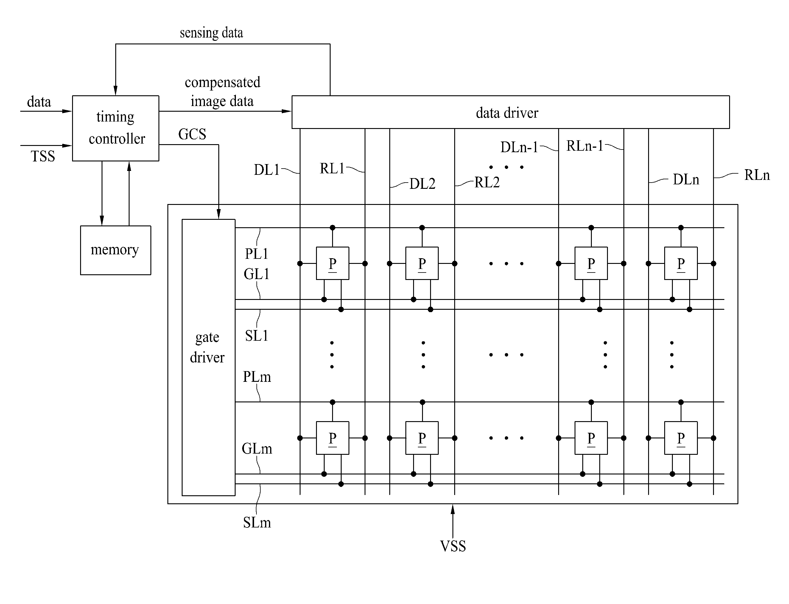
Thin film transistor of display apparatus
a technology of display apparatus and thin film, which is applied in the direction of transistors, electrical appliances, semiconductor devices, etc., can solve the problems of screen defect and screen defect, and achieve the effects of reducing leakage current, and preventing a screen defect of the display apparatus
- Summary
- Abstract
- Description
- Claims
- Application Information
AI Technical Summary
Benefits of technology
Problems solved by technology
Method used
Image

Examples
first embodiment
[0096]FIG. 6 illustrates a plan layout of a TFT 100 according to the present invention and is a diagram illustrating a plan layout of a pull-down TFT among a plurality of buffer TFTs included in a scan circuit of a gate driver. FIG. 8A is a diagram illustrating a cross-sectional surface of a pull-down TFT taken along lines B1-B2 and C1-C2 of FIG. 6.
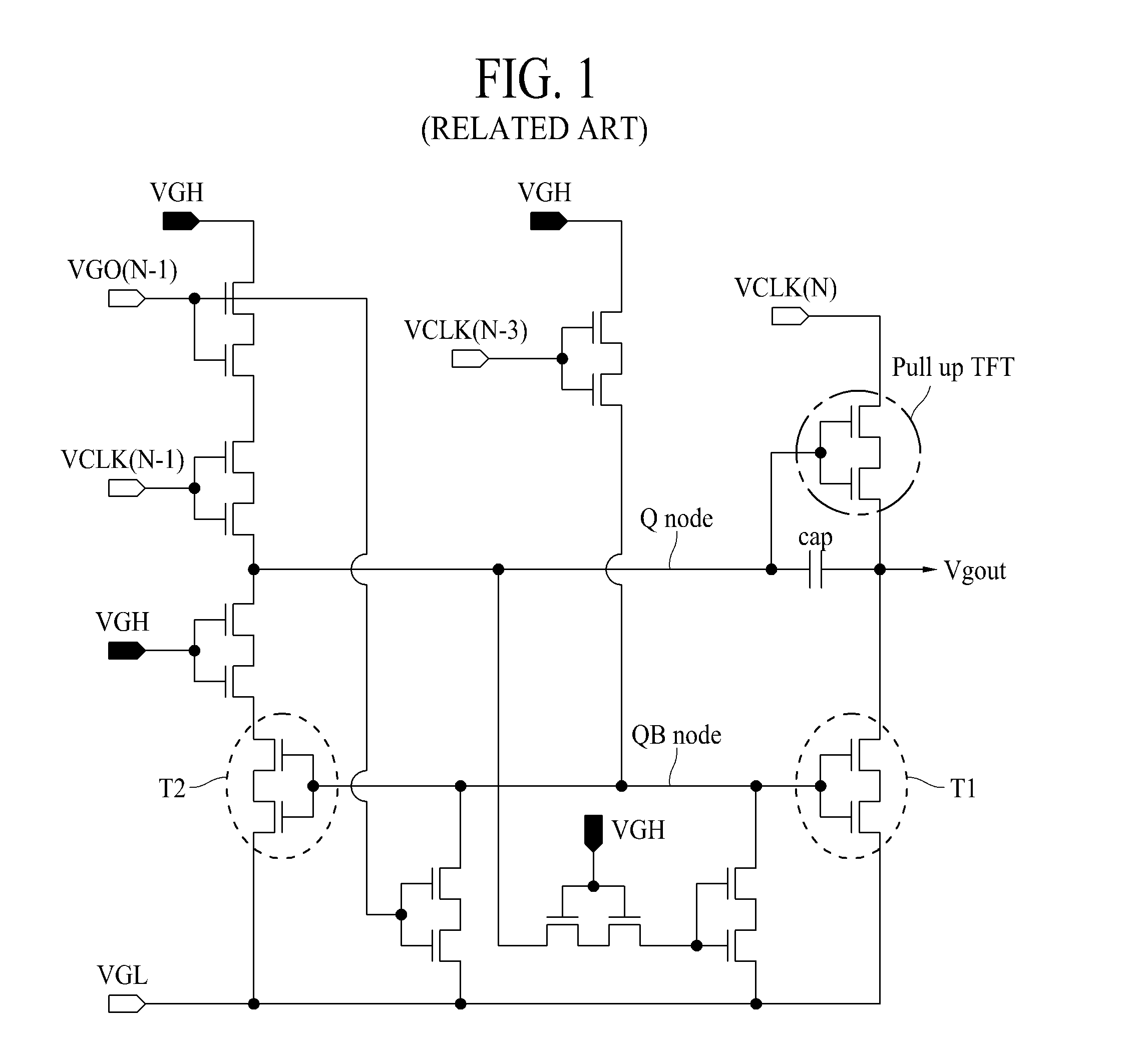
[0097]Referring to FIGS. 6 and 8A, the TFT 100 according to the first embodiment of the present invention may be applied to a plurality of buffer TFTs (a pull-up TFT and a pull-down TFT) of a scan circuit. Hereinafter, an example where the TFT 100 according to the first embodiment of the present invention is applied to a pull-down TFT (T1 of FIG. 1) among the buffer TFTs of the scan circuit will be described.
[0098]The pull-down TFT of the scan circuit may be implemented to have a larger area than those of general switching TFTs so as not to be deteriorated by a high voltage and long-time driving. In the TFT 100 according to the first embo...
second embodiment
[0121]FIG. 7 illustrates a plan layout of a TFT 100 according to the present invention and is a diagram illustrating a plan layout of a pull-down TFT among a plurality of buffer TFTs included in a scan circuit of a gate driver. FIG. 8B is a diagram illustrating a cross-sectional surface of a pull-down TFT taken along lines B1-B2 and D1-D2 of FIG. 7.
[0122]Referring to FIGS. 7 and 8B, in the TFT 100 according to the second embodiment of the present invention, a gate electrode 120 may be formed in a double line structure for forming a multichannel, and an active layer 110 may be patterned for forming a plurality of channels.
[0123]The gate electrode 120 may branch as two lines from a gate line and may be long formed in a horizontal direction. With respect to a plane, a source electrode 130 may be disposed under the gate electrode 120, and a drain electrode 140 may be disposed on the gate electrode 120. The active layer 110 may be disposed to overlap the gate electrode 120 and may contac...
third embodiment
[0140]FIG. 9 illustrates a plan layout of a TFT 200 according to the present invention and is a diagram illustrating a plan layout of a switching TFT, included in a scan circuit of a gate driver, or a switching TFT included in a pixel circuit. FIG. 11A is a diagram illustrating a cross-sectional surface, taken along line E1-E2 of FIG. 9, of a switching TFT included in a scan circuit or a switching TFT included in a pixel circuit.
[0141]Referring to FIGS. 9 and 11A, the TFT 200 according to the third embodiment of the present invention may be applied to a switching TFT (T2 (a reset TFT) of FIG. 1) of a scan circuit. The switching TFT of the scan circuit should quickly operate in response to an input signal and thus may be formed to have a smaller area than that of a buffer TFT. Also, the TFT 200 according to a third embodiment of the present invention may be applied to a switching TFT of a pixel circuit. The switching TFT of the pixel circuit should quickly operate in response to an i...
PUM
 Abstract
Description
Claims
Application Information