

Light emitting device
A light-emitting device and light-emitting layer technology, which is applied in the manufacture of electric solid-state devices, semiconductor devices, semiconductor/solid-state devices, etc., can solve the problems of the allowable number of defects being reduced, and achieve the effects of reducing electric power, reducing dark spots, and reducing driving voltage
- Summary
- Abstract
- Description
- Claims
- Application Information
AI Technical Summary
Problems solved by technology
Method used
Image

Examples
specific example
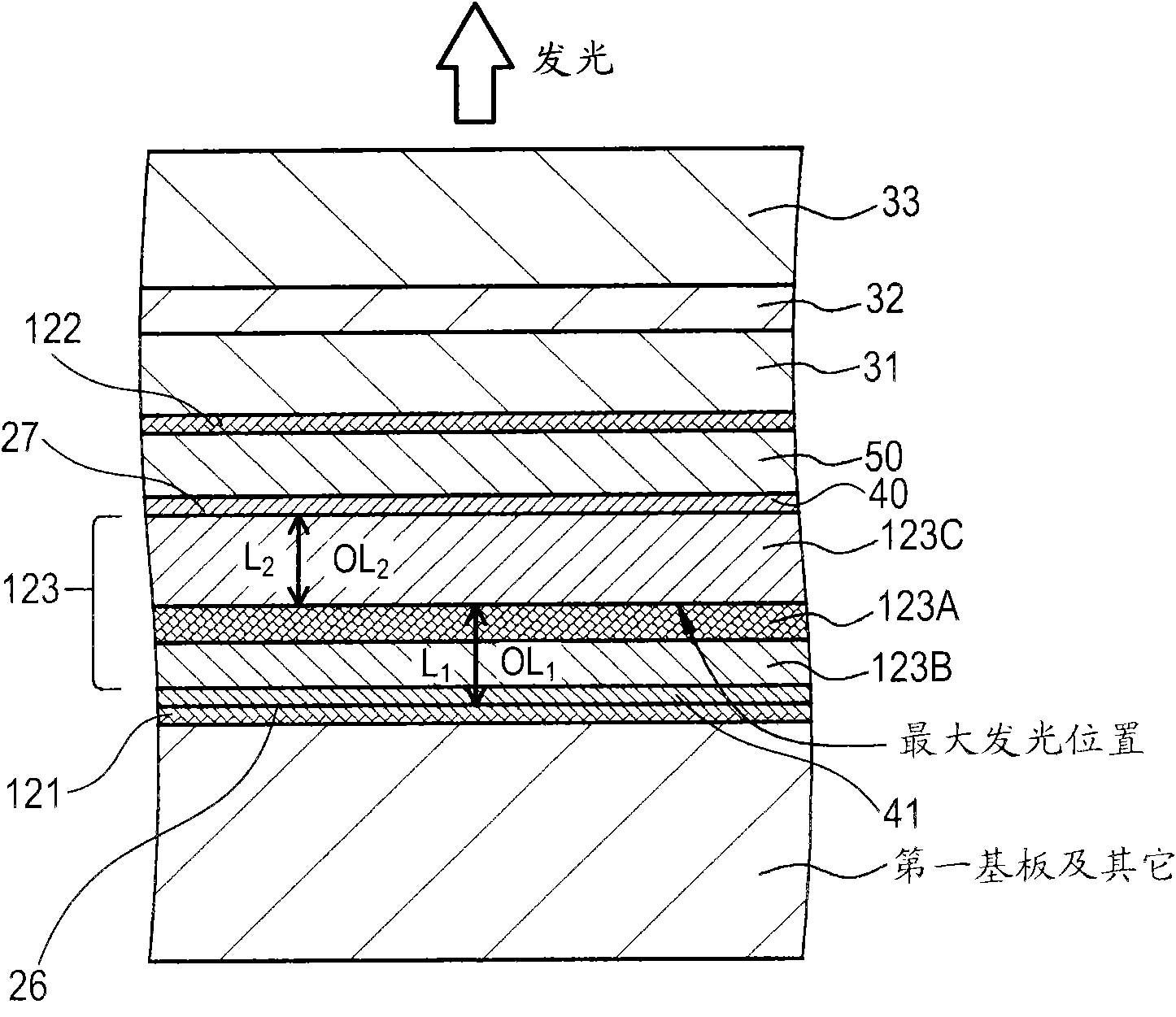
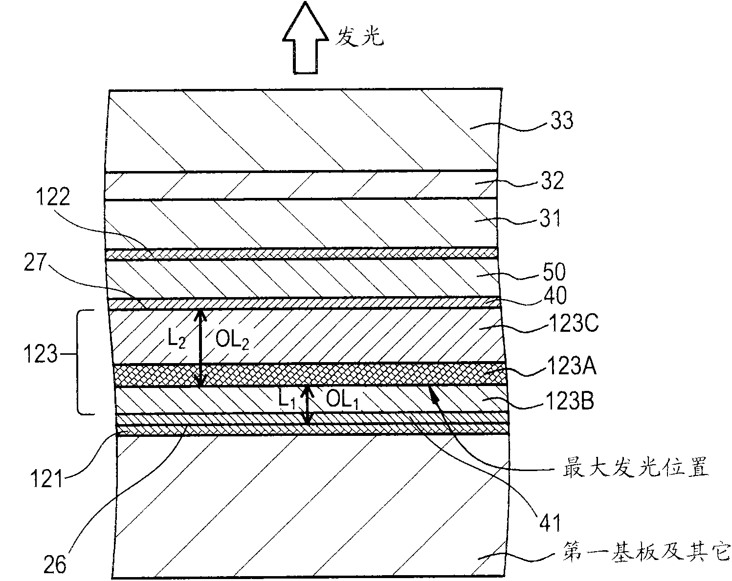
[0145] In the organic EL display device, a configuration may be formed in which a second substrate fixed over a second electrode is provided. There may be cases where an organic EL display device of such a configuration is referred to as a "top emission type organic EL display device" for convenience. On the other hand, it is also possible to form a configuration in which the first substrate fixed below the second electrode is provided. There may be cases where an organic EL display device of such a configuration is referred to as a "bottom emission type organic EL display device" for convenience. In the top emission type organic EL display device, a mode may be formed in which a protective film and an adhesive layer (sealing layer) are formed between the second electrode and the second substrate from the second electrode side. Here, as a material constituting the protective film, preferably, a material that is transparent to light emitted in the light emitting layer, is minu...
Embodiment 1
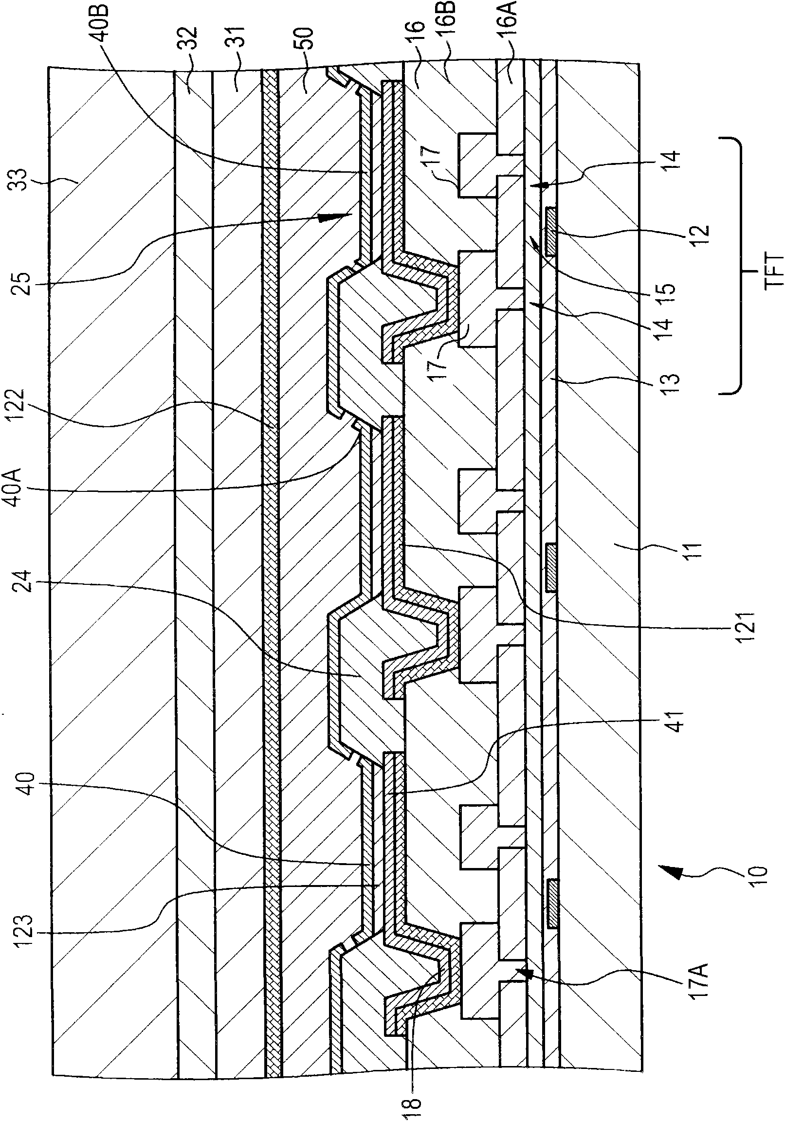
[0155] Example 1 relates to the light emitting device according to the first embodiment of the present invention. figure 1 shows a schematic partial cross-sectional view of an organic EL display device to which the light emitting device according to the first embodiment of the present invention is applied; Figure 2A and Figure 2B Each shows a schematic diagram of an organic layer and the like. The organic EL display device in Example 1 is an active matrix type organic EL display device for color display, and is of a top emission type. That is, light passes through the second electrode, and is further output through the second substrate.
[0156] The organic EL display device in Embodiment 1 has a plurality (for example, N×M=2880×540) of light-emitting devices (specifically, organic EL devices) 10 . A single light emitting device (organic EL device) 10 constitutes a single sub-pixel. Therefore, the organic EL display device has (N×M) / 3 pixels. Here, a single pixel is co...
Embodiment 2
[0262] Embodiment 2 is related to a modification of Embodiment 1, and the resistance layer has a structure in which the first resistance layer and the second resistance layer are laminated from the organic layer side, and the resistivity of the second resistance layer is higher than that of the first resistance layer. A resistive layer has a high resistivity. In Embodiment 2, the material constituting each of the first resistance layer and the second resistance layer is Nb 2 o 5 , and by sputtering the Nb 2 o 5 Change the oxygen partial pressure during film deposition to adjust the resistivity R of the first resistive layer and the second resistive layer respectively 1 and R 2 ,As follows.
[0263] The resistivity R of the first resistive layer 1 : 1×10 6 Ω m (1×10 4 Ω·cm)
[0264] The resistivity R of the second resistive layer 2 : 1×10 8 Ω m (1×10 6 Ω·cm)
[0265] When measuring the voltage drop in the resistive layer, it is the same as when the resistive layer ...
PUM
 Abstract
Description
Claims
Application Information