Photoelectric conversion apparatus

a conversion apparatus and photoelectric technology, applied in the direction of solid-state devices, instruments, material analysis, etc., can solve the problems of insufficient carrier injection from the emitter to the collector, low current amplification ratio, and degraded photoelectric conversion characteristics at low-light intensity

Inactive Publication Date: 2012-07-12
CANON KK
View PDF1 Cites 23 Cited by
  • Summary
  • Abstract
  • Description
  • Claims
  • Application Information

AI Technical Summary

Problems solved by technology

Accordingly, the recombination current component between the base and the emitter of the phototransistor is the main component of the current, thus causing insufficient carrier injection from the emitter to the collector.
As a result, the current amplification ratio decreases and the photoelectric conversion characteristics at low-light intensity degrade.
Unfortunately, Japanese Patent Application Laid-Open No.
H08-264744 does not disclose a means of determining the value of the current to flow through the base, and hence has a problem in that an appropriate carrier cannot be injected when the current amplification ratio of the phototransistor decreases.
H08-264744 has another problem in that an appropriate carrier cannot be injected into an individual phototransistor greatly affected by manufacturing variations due to pixel multiplication and microminiaturization of the phototransistor.

Method used


Image

  • Photoelectric conversion apparatus
  • Photoelectric conversion apparatus
  • Photoelectric conversion apparatus

Examples


first embodiment

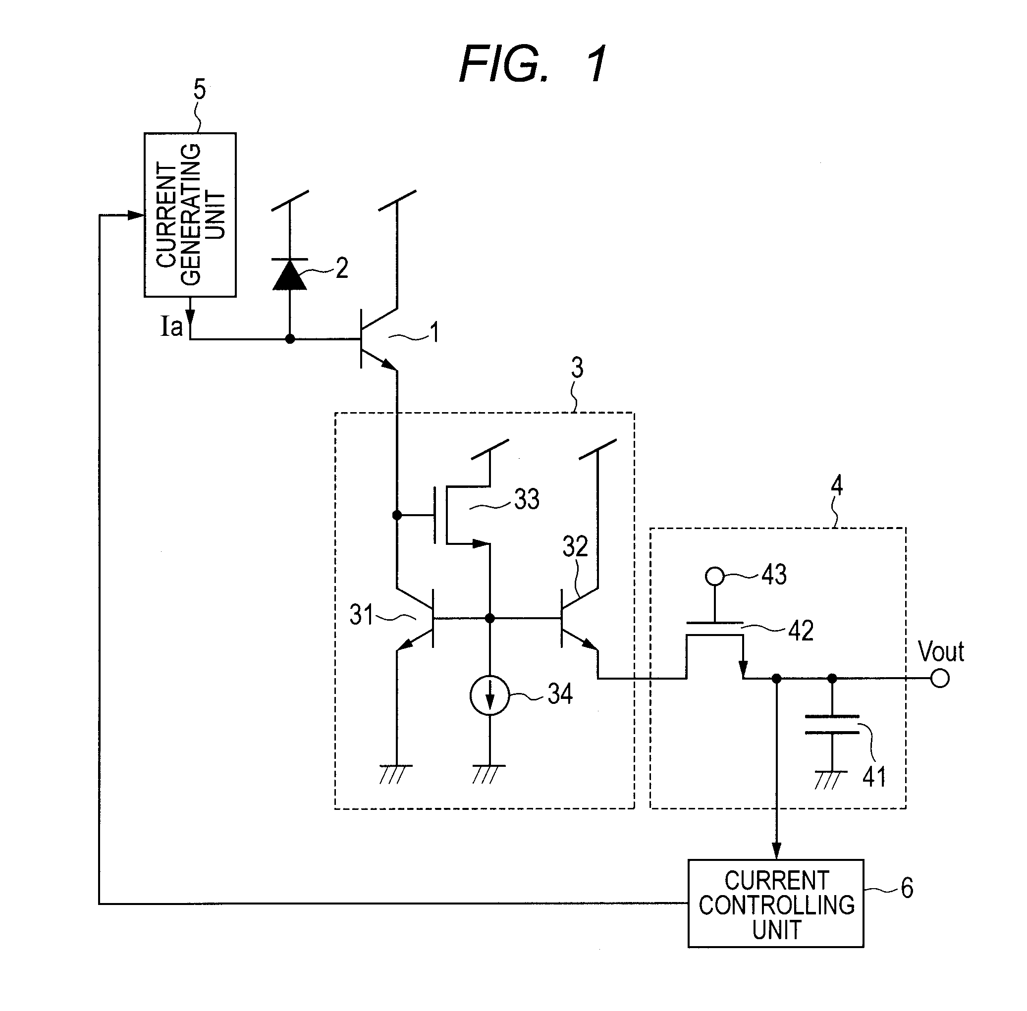
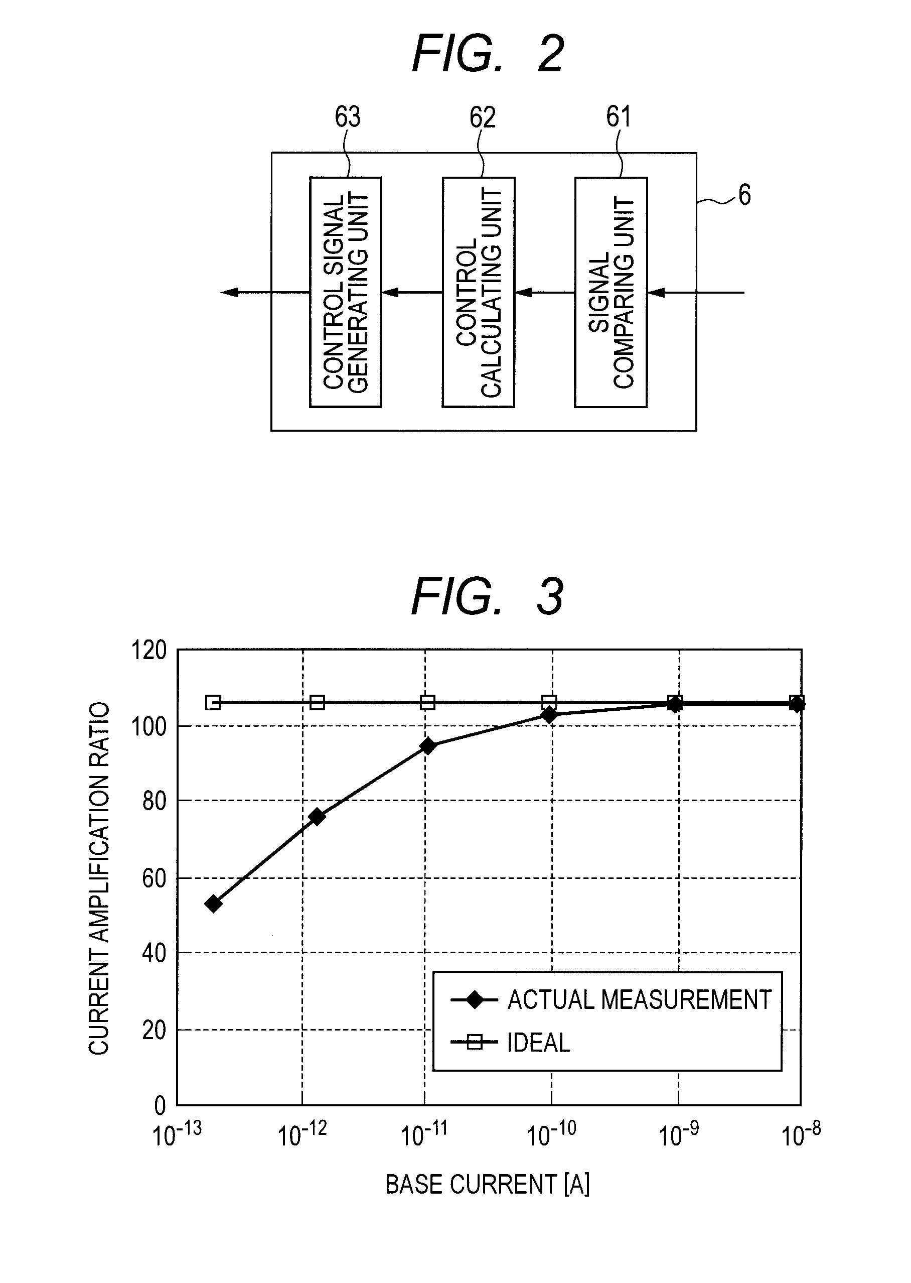
[0018]FIG. 1 is a schematic configuration view illustrating a photoelectric conversion apparatus according to a first embodiment of the present invention. FIG. 1 includes a phototransistor 1, and a photoelectric conversion element 2 (e.g., photodiode), where its cathode is connected to a power supply voltage node. The phototransistor 1 is configured such that its base is connected to the anode of the photoelectric conversion element 2 and its collector is connected to the power supply voltage node. The photoelectric conversion element 2 converts light to an electrical signal by photoelectric conversion to generate a current (photocurrent). The phototransistor 1 inputs from the base thereof the current generated by the photoelectric conversion element 2, amplifies the input current, and outputs the amplified current from the emitter. FIG. 1 further includes a logarithmic conversion unit 3 that includes transistors 31, 32, and 33, and a constant current source 34. The bipolar transist...

second embodiment

[0027]FIG. 5 is a configuration example of a current generating unit 5 according to a second embodiment of the present invention. FIG. 5 illustrates an embodiment describing the current generating unit 5 in FIG. 1 further in detail. The phototransistor 1, the photoelectric conversion element 2, the logarithmic conversion unit 3, the signal accumulation unit 4, and the current controlling unit 6 in FIG. 5 are the same as those in FIG. 1. The current generating unit 5 includes a resistor element 55 and a voltage source 56. One end of the resistor element is electrically connected to the base of the photoelectric conversion element 2 and the phototransistor 1; and the other end thereof is connected to the voltage node of the voltage Va. The voltage source 56 generates the voltage Va by the control of the current controlling unit 6. Specifically, the voltage source 56 supplies the resistor element 55 with an appropriate voltage Va required to generate a current Ia to be added to the bas...

third embodiment

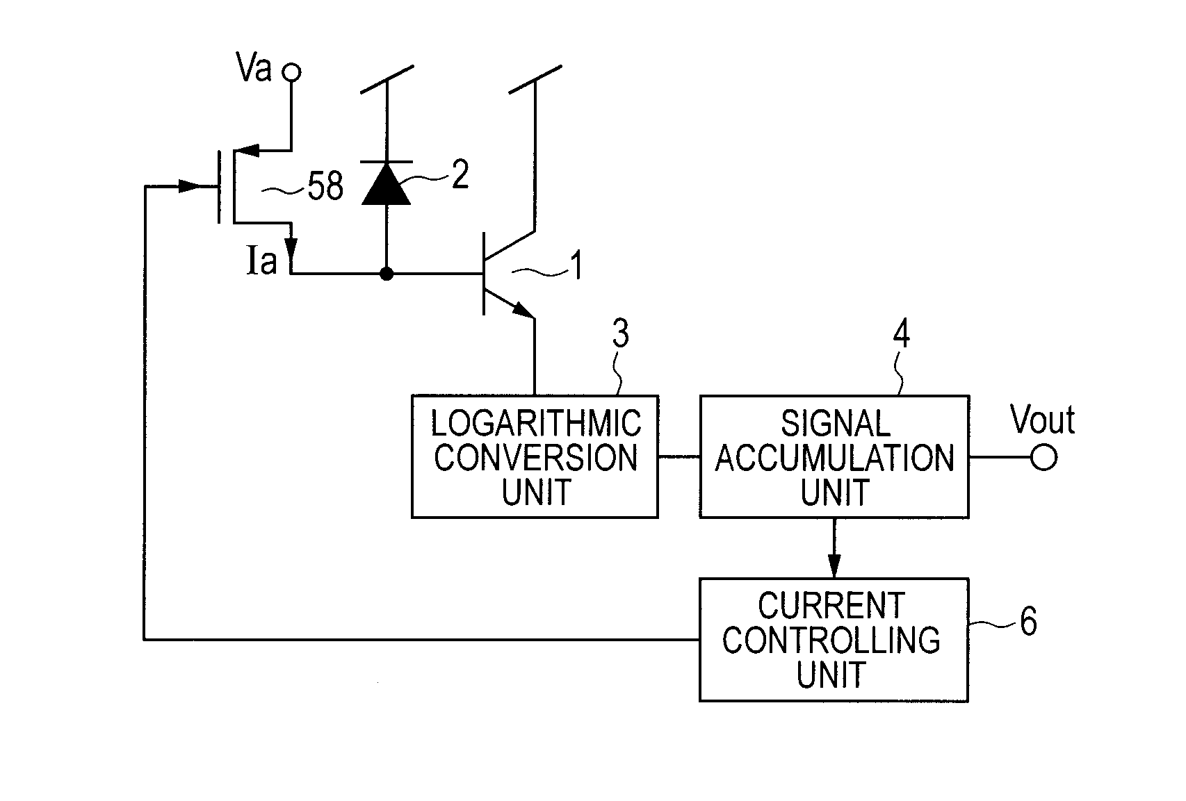
[0028]FIG. 6 is a configuration example of a current generating unit 5 according to a third embodiment of the present invention. FIG. 6 illustrates an embodiment describing the current generating unit 5 in FIG. 1 further in detail. The phototransistor 1, the photoelectric conversion element 2, the logarithmic conversion unit 3, the signal accumulation unit 4, and the current controlling unit 6 in FIG. 6 are the same as those in FIG. 1. The current generating unit 5 includes a variable resistor element 57. One end of the variable resistor element 57 is electrically connected to the base of the photoelectric conversion element 2 and the phototransistor 1; and the other end thereof is electrically connected to the node of a constant voltage Va such as the voltage source. The resistor value of the variable resistor element 57 is controlled by the current controlling unit 6, and thereby the current Ia to be added to the base of the phototransistor 1 can be controlled. Thus, in a case in ...


PUM


Abstract

There is provided a photoelectric conversion apparatus capable of obtaining good photoelectric conversion characteristics regardless of a decrease in current amplification ratio of the phototransistor and manufacturing variations in phototransistor. The photoelectric conversion apparatus includes a photoelectric conversion element that generates a current by photoelectric conversion; a transistor that inputs a current generated by the photoelectric conversion element to a base thereof, amplifies the input current, and outputs the amplified current from an emitter; a logarithmic conversion unit that logarithmically converts the current output from the transistor; a current generating unit that outputs the current to the base of the transistor; and a current controlling unit that controls the output current of the current generating unit in a light shielding state of the photoelectric conversion element based on the signal logarithmically converted by the logarithmic conversion unit.

Description

BACKGROUND OF THE INVENTION[0001]1. Field of the Invention[0002]The present invention relates to a photoelectric conversion apparatus.[0003]2. Description of the Related Art[0004]There has conventionally been disclosed a photoelectric conversion apparatus that receives light in the base of a phototransistor and outputs an amplified photocurrent from the emitter (for example, see Japanese Patent Application Laid-Open No. 2000-077644). In the case of low-light intensity, the phototransistor generates a slight base current. Accordingly, the recombination current component between the base and the emitter of the phototransistor is the main component of the current, thus causing insufficient carrier injection from the emitter to the collector. As a result, the current amplification ratio decreases and the photoelectric conversion characteristics at low-light intensity degrade. In order to solve this problem, there has been disclosed a photoelectric conversion apparatus that injects a car...

Claims


Application Information

Patent Timeline
Patent Type & Authority Applications(United States)
IPC IPC(8): H01L31/02
CPCH01L27/14623H01L27/14609
Inventor KURODA, YUKIHIROKOBAYASHI, HIDEO
Owner CANON KK
Why Eureka
Try Eureka