Switch circuit capable of preventing voltage spike, and control method and layout structure thereof

a technology of switching circuit and voltage spike, which is applied in the direction of electronic switching, pulse technique, semiconductor devices, etc., can solve the problems of affecting the stability of the circuit, so as to reduce the variation of input current and prevent the voltage spike

Inactive Publication Date: 2012-07-12
ANPEC ELECTRONICS CORPORATION
View PDF4 Cites 6 Cited by
  • Summary
  • Abstract
  • Description
  • Claims
  • Application Information

AI Technical Summary

Benefits of technology

[0008]The present invention discloses a switch circuit capable of preventing voltage spike, which includes an input end for receiving an input voltage; an output end for outputting an output voltage; a switch unit coupled to the input end and the output end for controlling an electrical connection between the input end and the output end according to a control signal; a protection unit coupled to the input end for generating the control signal according to an input current passing through the input end; and a first parasitic transistor comprising a first end coupled to the protection unit for receiving the control signal, a second end coupled to the input end, and a third end coupled to a reference potential end for controlling an electrical connection between the second end and the third end according to the control signal; wherein when the input current is greater than a threshold value, the switch unit turns off the electrical connection between the input end and the output end according to the control signal, and the first parasitic transistor turns on the electrical connection between the second end and the third end of the first parasitic transistor according to the control signal to reduce variation of the input current.
[0009]The present invention further discloses a control method capable of preventing voltage spike for a switch unit, the switch unit receiving an input voltage via an input end and outputting an output voltage via an output end, the control method includes turning off an electrical connection between the input end and the output end when an input current passing through the input end is greater than a threshold value; and turning on a first parasitic transistor so that the input current is capable of passing through the first parasitic transistor to create a current path for reducing variation of the input current.

Problems solved by technology

In other words, the input current IIN would become extremely large, damaging the internal components of the electronic product 100 or the power system 10.
However, in practice, a circuit response period is required for the over-current protection scheme to initial current limiting function when an over-current situation occurs.
Since the input current IIN have great current variation, the input voltage VIN would be sharply pulled up to maintain the continuity of the inductor current so that a serious voltage ripple effect occurs, also damaging the internal components of the electronic product 100 or the power system 10.

Method used


Image

  • Switch circuit capable of preventing voltage spike, and control method and layout structure thereof
  • Switch circuit capable of preventing voltage spike, and control method and layout structure thereof
  • Switch circuit capable of preventing voltage spike, and control method and layout structure thereof

Examples


Embodiment Construction

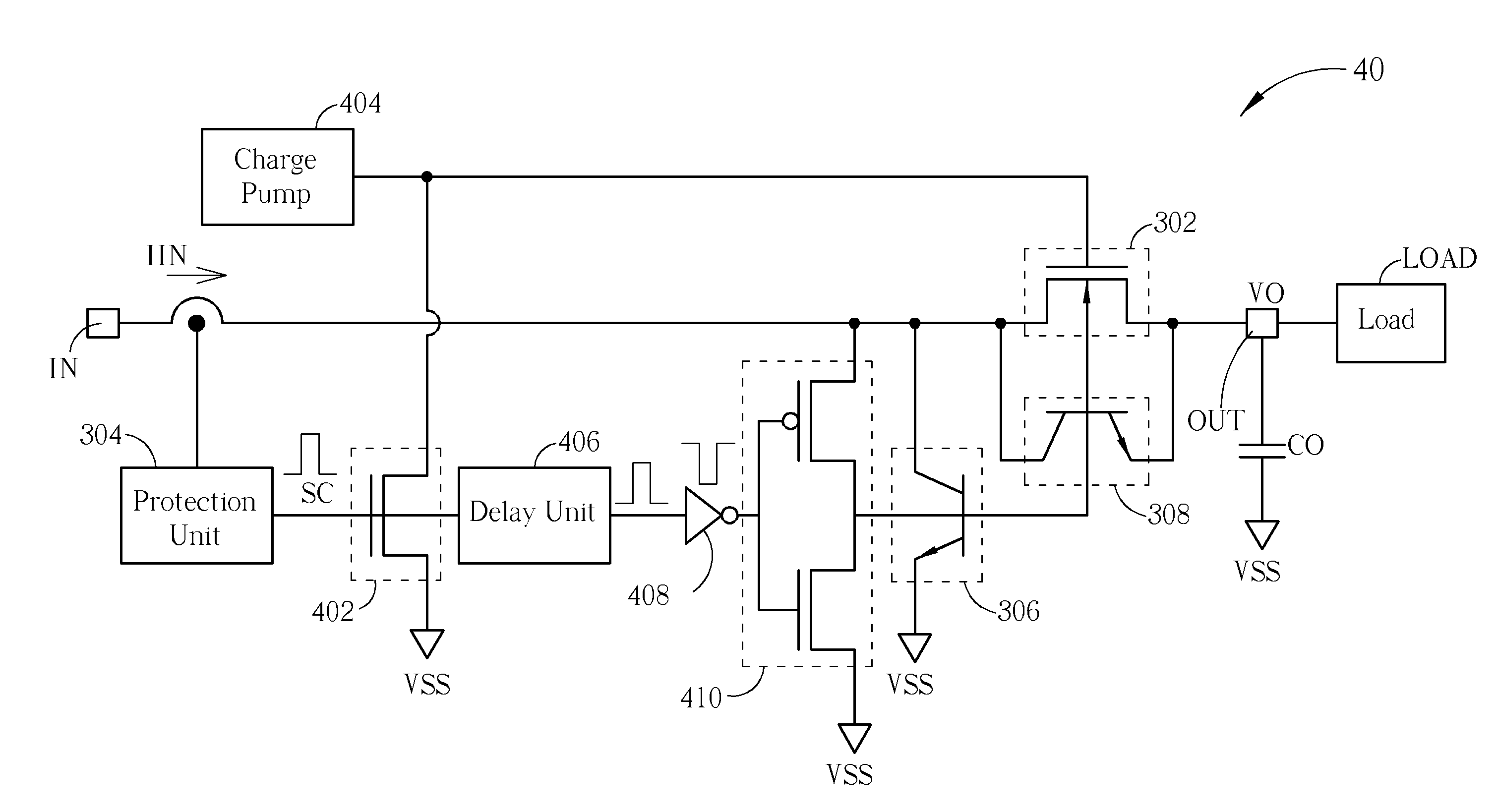
[0019]Please refer to FIG. 3, which illustrates a schematic diagram of a switch circuit 30 according to an embodiment of the present invention. The switch circuit 30 is utilized for receiving an input voltage VIN and outputting an output voltage VO to a load LOAD. The switch circuit 30 includes an input end IN, an output end OUT, a switch unit 302, a protection unit 304, a first parasitic transistor 306, a second parasitic transistor 308, and an output capacitor CO. The input end IN is utilized for receiving the input voltage VIN. The output end OUT is utilized for outputting the output voltage VO. The switch unit 302 is coupled to the input end VIN and the output end OUT for controlling an electrical connection between the input end IN and the output end OUT according to a control signal SC. In other words, the switch unit 302 can control the electrical connection between the input end IN and the output end OUT according to circuit system requirement during normal operation, and fu...


PUM


Abstract

A switch circuit capable of preventing voltage spike, includes an input end for receiving an input voltage, an output end for outputting an output voltage, a switch unit for controlling an electrical connection between the input end and the output end according to a control signal, a protection unit for generating the control signal according to an input current passing through the input end, and a first parasitic transistor for controlling an electrical connection between a second end and a third end according to the control signal, wherein when the input current is greater than a threshold value, the switch unit turns off electrical connection between the input end and the output end according to the control signal, and the first parasitic transistor turns on electrical connection between the second end and the third end of first parasitic transistor according to the control signal to reduce variation of input current.

Description

BACKGROUND OF THE INVENTION[0001]1. Field of the Invention[0002]The present invention relates to a switch circuit and related control method and layout structure, and more particularly, to a switch circuit capable of preventing voltage spike and related control method and layout structure.[0003]2. Description of the Prior Art[0004]In general, power supplies are required for all electronic products to offer operating energy. Please refer to FIG. 1, which illustrates a schematic diagram of a power system 10 according to the prior art. In the power system 10, a power supply 102 is utilized for providing an input voltage VIN (not shown in FIG. 1). A switch circuit 104 receives an input voltage VIN via an input end IN and further controls whether to output an output voltage VO to an electronic product 100. However, since a short circuit condition occurs in the switch circuit 104, large short current may be introduced instantaneously. In other words, the input current IIN would become ext...

Claims


Application Information

Patent Timeline
Patent Type & Authority Applications(United States)
IPC IPC(8): H03K17/687H01L27/06
CPCH01L27/027H03K17/567H03K17/0828H01L27/088
Inventor YANG, TSE-LUNGCHANG, HSIANG-CHUNG
Owner ANPEC ELECTRONICS CORPORATION
Why Eureka
Try Eureka