Arrayed waveguide grating type optical multiplexer and demultiplexer

a waveguide and optical multiplexer technology, applied in the field of array waveguide grating type optical multiplexer and demultiplexer, can solve the problems of increasing the size of the package, and increasing the number of components

Inactive Publication Date: 2012-08-02
FURUKAWA ELECTRIC CO LTD
View PDF6 Cites 33 Cited by
  • Summary
  • Abstract
  • Description
  • Claims
  • Application Information

AI Technical Summary

Benefits of technology

[0076]Next, the operation of the arrayed waveguide grating type optical multiplexer and demultiplexer 1 will be explained.
[0077]When the arrayed waveguide grating type optical multiplexer and demultiplexer 1 is used for multiplexing (MUX), in each of the waveguide chips 16, as shown in FIG. 1A by the arrow A, plural optical signals having respective wavelengths different from one another (λ1 to λn) are input individually from the second waveguides 24.
[0078]The input optical signals (λ1 to λn) are input individually into the respective channel waveguides 28a in the arrayed waveguide grating 14 through the second slab waveguide 26.
[0079]The optical signals (λ1 to λn) propagated in the respective channel waveguides 28a are multiplexed in the first slab waveguide 22 and output from the first waveguide 20 as a wavelength multiplexed optical signal as shown in FIG. 1A by the arrow B.
[0080]Here, when temperature changes, a light collection position of the first slab waveguide 22 (light collection position of the second separated slab waveguide 22B in the first

Problems solved by technology

Along with a higher functionality of the recent wavelength multiplexer and demultiplexer, the number of components to be included in a package tends to be increased and there is a problem that a package size

Method used


Image

  • Arrayed waveguide grating type optical multiplexer and demultiplexer
  • Arrayed waveguide grating type optical multiplexer and demultiplexer
  • Arrayed waveguide grating type optical multiplexer and demultiplexer

Examples


embodiment 1

1. Embodiment 1

[0050]Preferred embodiments of the present invention will now be described in detail in accordance with the accompanying drawings.

[0051]In the following, an example of an arrayed waveguide grating type optical multiplexer and demultiplexer according to the present invention will be explained.

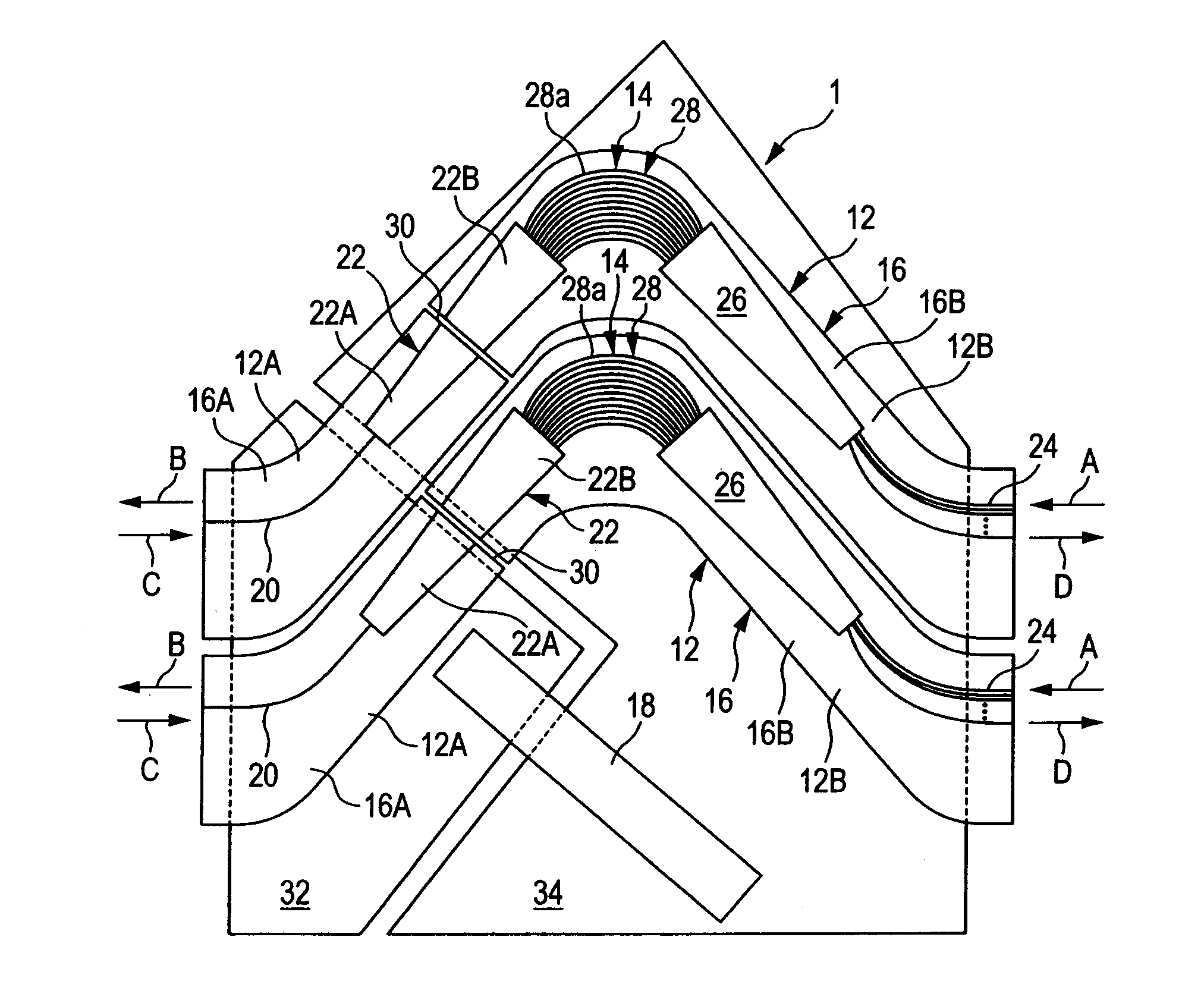
[0052]FIG. 1A and FIG. 1B show a plan view and a side view of an arrayed waveguide grating type optical multiplexer and demultiplexer 1 according to Embodiment 1, respectively. The arrayed waveguide grating type optical multiplexer and demultiplexer 1 includes a waveguide chip 16 on which an arrayed waveguide grating 14 is formed, bases 32 and 34, and a compensation member 18.

[0053]The waveguide chip 16 includes a substrate 12 made of silicon and the two arrayed waveguide gratings 14 formed on the substrate 12 and provided in parallel to each other, and has an approximately boomerang-like planar shape cut in a curved shape along the outline of the arrayed waveguide grating 14. The...

embodiment 2

2. Embodiment 2

[0094]In the following, another example of the arrayed waveguide grating type optical multiplexer and demultiplexer according to the present invention will be explained.

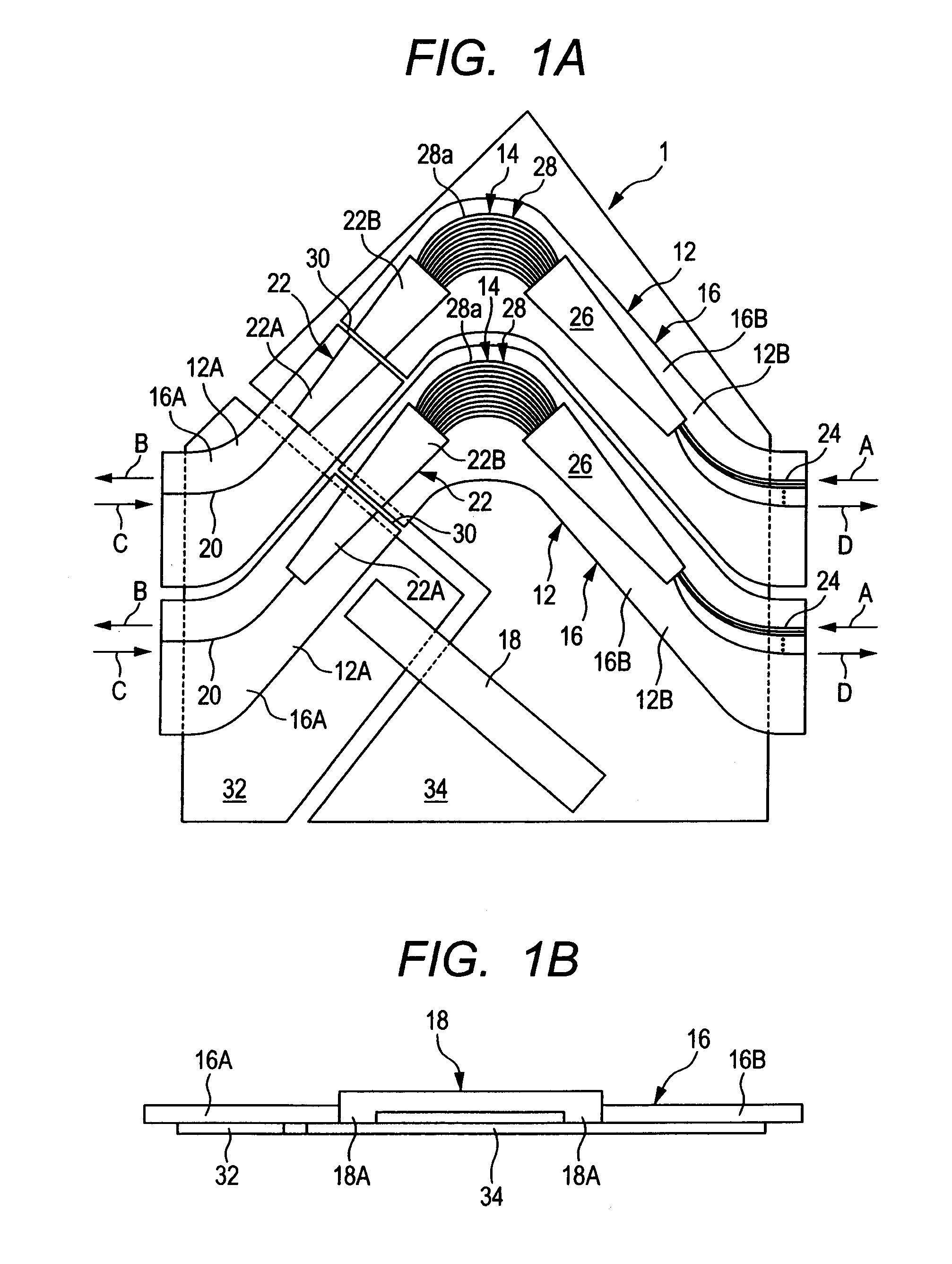
[0095]FIG. 2A and FIG. 2B show a plan view and a side view of an arrayed waveguide grating type optical multiplexer and demultiplexer 2 according to Embodiment 2, respectively. The arrayed waveguide grating type optical multiplexer and demultiplexer 2 according to Embodiment 2 includes two arrayed waveguide gratings 14 provided in parallel to each other as same as Embodiment 1. Note that the number of the arrayed waveguide gratings 14 is not limited to two and may be three or larger.

[0096]As shown in FIG. 2A, the waveguide chip 16 is cut by one cut plane 30 in a part for respective first slab waveguides 22 in the two arrayed waveguide gratings 14 and divided into a first separated waveguide chip 16A and a second separated waveguide chip 16B. Accordingly, the first slab waveguide 22 is also separated by...

embodiment 3

3. Embodiment 3

[0108]In the following, still another example of the arrayed waveguide grating type optical multiplexer and demultiplexer according to the present invention will be explained.

[0109]FIG. 3A and FIG. 3B show a plan view and a side view of an arrayed waveguide grating type optical multiplexer and demultiplexer 3 according to Embodiment 3, respectively. The arrayed waveguide grating type optical multiplexer and demultiplexer 3 according to Embodiment 3, as with Embodiment 1, includes two arrayed waveguide gratings 14 provided in parallel to each other. Note that the number of the arrayed waveguide gratings 14 is not limited to two and may be three or larger.

[0110]As shown in FIG. 3A, a waveguide chip 16, as with Embodiment 2, is cut by one cut plane 30 in a part for respective first slab waveguides 22 in the two arrayed waveguide gratings 14 and divided into a first separated waveguide chip 16A and a second separated waveguide chip 16B. Accordingly, the first slab wavegui...


PUM


Abstract

An arrayed waveguide grating type optical multiplexer and demultiplexer which reduces a package size although plural arrayed waveguide gratings are included, is provided, comprising plural arrayed waveguide gratings which are provided in parallel to one another on a substrate and each of which has a first waveguide, a first slab waveguide, an arrayed waveguide, a second slab waveguide, and a second waveguide, and also includes a waveguide chip divided into a first and second separated waveguide chip in the first or second slab waveguide in each of the arrayed waveguide gratings and a compensation member compensating a temperature dependent shift of a light transmission center wavelength in the arrayed waveguide grating by relatively moving the first and second waveguide chip when expanded or contracted according to a temperature change. The waveguide chip has a shape bending along a bending direction of the arrayed waveguide.

Description

CROSS-REFERENCE TO RELATED APPLICATIONS[0001]This application is a continuation of International Application No. PCT / JP2011 / 064400, filed Jun. 23, 2011, which claims the benefit of Japanese Patent Application No. 2010-152244, filed Jul. 2, 2010. The contents of the aforementioned applications are incorporated herein by reference in their entities.BACKGROUND OF THE INVENTION[0002]1. Field of the Invention[0003]The present invention relates to an arrayed waveguide grating type optical multiplexer and demultiplexer having a function of a wavelength multiplexer and demultiplexer which unifies light beams having respective wavelengths different from one another and separates a light beam for each of the wavelengths, and specifically relates to an arrayed waveguide grating type optical multiplexer and demultiplexer which is made athermal (temperature independent).[0004]2. Description of the Related Art[0005]In an arrayed waveguide grating (AWG) playing an important role as a wavelength mu...

Claims


Application Information

Patent Timeline
IPC IPC(8): G02B6/34
CPCG02B6/12014
Inventor HASEGAWA, JUNICHINARA, KAZUTAKA
Owner FURUKAWA ELECTRIC CO LTD
Why Eureka
Try Eureka