

Voltage regulator
a voltage regulator and ripple rejection technology, applied in the direction of electric variable regulation, process and machine control, instruments, etc., can solve the problem that conventional technology is unsuitable for mass production, and achieve the effect of low power consumption, simple configuration, and high ripple rejection ratio
- Summary
- Abstract
- Description
- Claims
- Application Information
AI Technical Summary
Benefits of technology
Problems solved by technology
Method used
Image

Examples
first embodiment
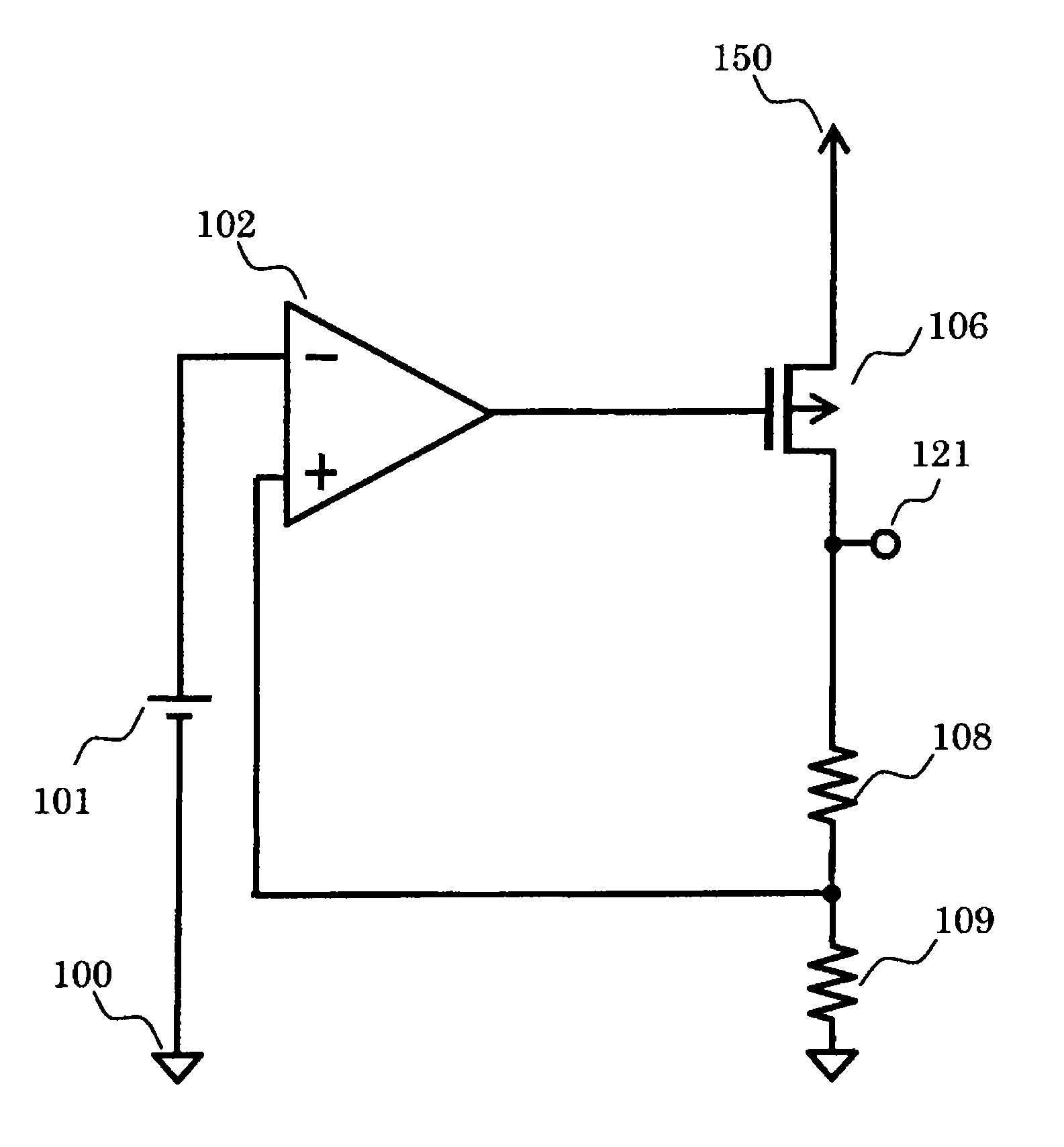
[0026]FIG. 1 is a circuit diagram of a voltage regulator according to the present invention. The voltage regulator includes a reference voltage circuit 101, a differential amplifier circuit (error amplifier circuit) 102, a PMOS transistor 106, resistors 108 and 109, a ground terminal 100, an output terminal 121, and a power supply terminal 150.
[0027]The error amplifier circuit 102 has an inverting input terminal connected to any one terminal of the reference voltage circuit 101, a non-inverting input terminal connected to a connection point between any one terminal of the resistor 108 and any one terminal of the resistor 109, and an output terminal connected to a gate of the PMOS transistor 106. Another terminal of the reference voltage circuit 101 is connected to the ground terminal 100. The PMOS transistor 106 has a source connected to the power supply terminal 150, and a drain connected to the output terminal 121 and another terminal of the resistor 108. Another terminal of the r...
second embodiment
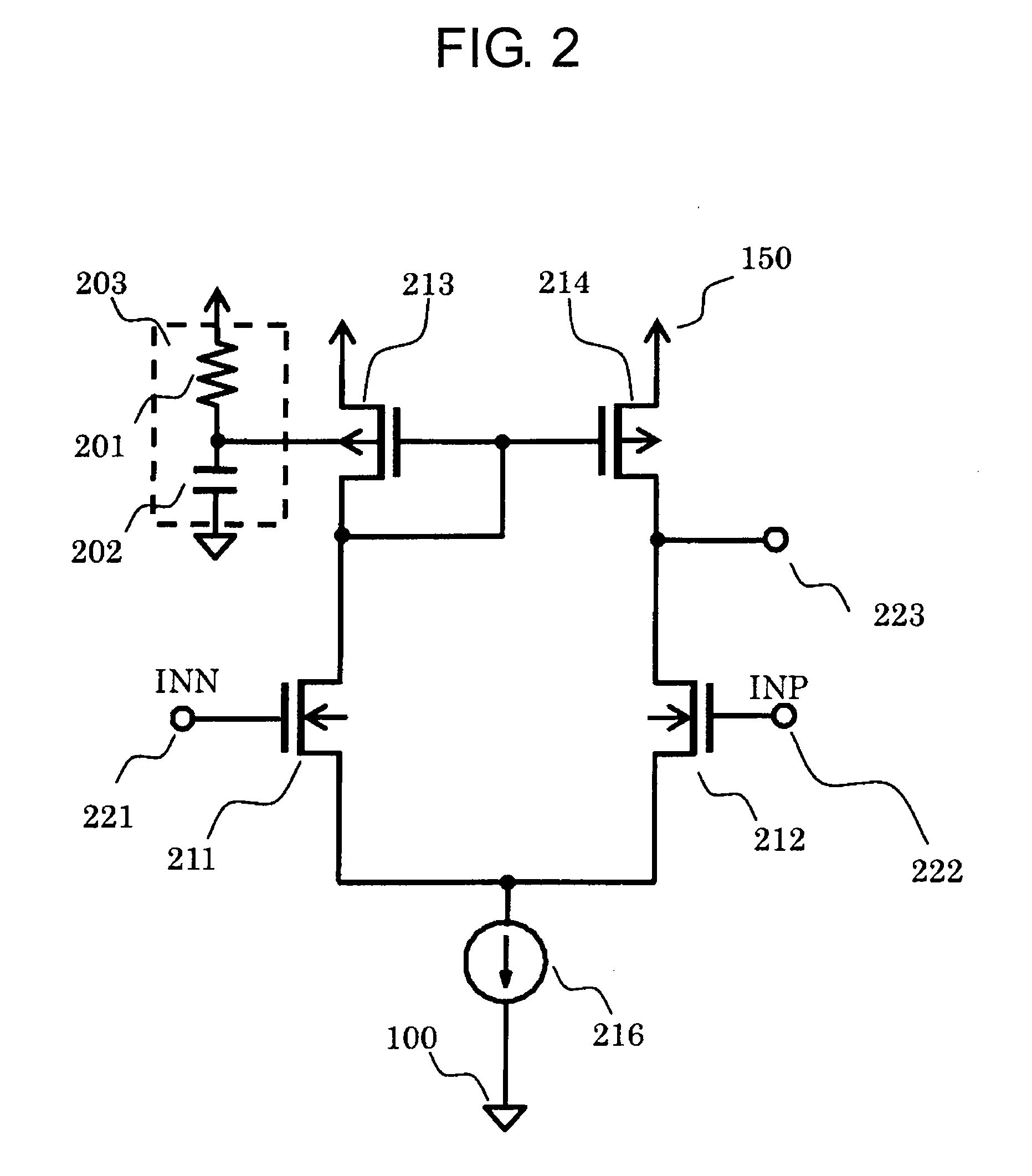
[0035]FIG. 4 is a circuit diagram of an error amplifier circuit 102 including a ripple rejection ratio improving circuit according to a second embodiment of the present invention. The second embodiment is different from the first embodiment in that an output of a ripple rejection ratio improving circuit 303 is input to a back gate of the NMOS transistor 211 that operates as an input stage transistor.
[0036]Connection is made as follows. A connection point between any one terminal of a resistor 301 and any one terminal of a capacitor 302 is connected to the back gate of the NMOS transistor 211. Another terminal of the resistor 301 is connected to the ground terminal 100. Another terminal of the capacitor 302 is connected to the power supply terminal 150. Other connection is the same as in the first embodiment illustrated in FIG. 2.
[0037]Next, an operation of the error amplifier circuit 102 according to the second embodiment is described.
[0038]The NMOS transistors 211 and 212 operate a...
third embodiment
[0041]FIG. 6 is a circuit diagram of an error amplifier circuit 102 including a ripple rejection ratio improving circuit according to a third embodiment of the present invention. The third embodiment is different from the first embodiment in that the error amplifier circuit has P-channel transistors as its inputs, and the connection of a ripple rejection ratio improving circuit 403 is changed.
[0042]A PMOS transistor 411 has a gate connected to an inverting input terminal 421, and a drain connected to a drain and a gate of an NMOS transistor 413 and a gate of an NMOS transistor 414. The PMOS transistor 411 has a source connected to any one terminal of a bias circuit 416 and a back gate connected to a connection point between any one terminal of a capacitor 402 and any one terminal of a resistor 401. Another terminal of the resistor 401 is connected to the source of the PMOS transistor 411. Another terminal of the capacitor 402 is connected to the power supply terminal 150. The NMOS t...
PUM
 Abstract
Description
Claims
Application Information