Packaging structure

a packaging structure and packaging technology, applied in the direction of semiconductor devices, semiconductor/solid-state device details, electrical devices, etc., can solve the problem of improper filling of underfill, and achieve the effect of reliable bonding effect and improved process yield

Inactive Publication Date: 2012-08-16
ADVANCED SEMICON ENG INC
View PDF12 Cites 13 Cited by
  • Summary
  • Abstract
  • Description
  • Claims
  • Application Information

AI Technical Summary

Benefits of technology

[0007]The present invention is directed to a package structure and a package process, wherein reliable bonding effect between an upper chip and through silicon vias of a chip carrier of a stacked semiconductor device package can be achieved to improve process yield.
[0008]The present invention is directed to a package structure and a package process, wherein a favorable gap between an upper chip and a molding compound of a stacked semiconductor device package can be effectively maintained for accomplishing a sequent molding process.
[0031]As to the above, pillar bumps are adopted in the present invention to connect an upper second chip and through silicon vias of a lower first chip so as to control a gap between the first chip and the second chip by adjusting a height of the pillar bumps. In other words, the pillar bumps of the present invention compensate the height difference between the first chip and a first molding compound surrounding the first chip so as to ensure the bondibility between the pillar bumps and the corresponding through silicon vias and thereby improve the process yield. Furthermore, the pillar bumps maintain the gap between the second chip and the first molding compound for allowing an underfill being properly filled into the space between the first chip and the second chip.

Problems solved by technology

If so, the height of bumps on the upper chip may not satisfy the aforementioned height difference as bonding the upper chip to the chip carrier, such that a failure of electrical test occurs due to invalid bonding between the bumps and the through silicon vias, or the underfill can not be properly filled into a restricted space between the upper chip and the molding compound.

Method used


Image

  • Packaging structure
  • Packaging structure
  • Packaging structure

Examples


Embodiment Construction

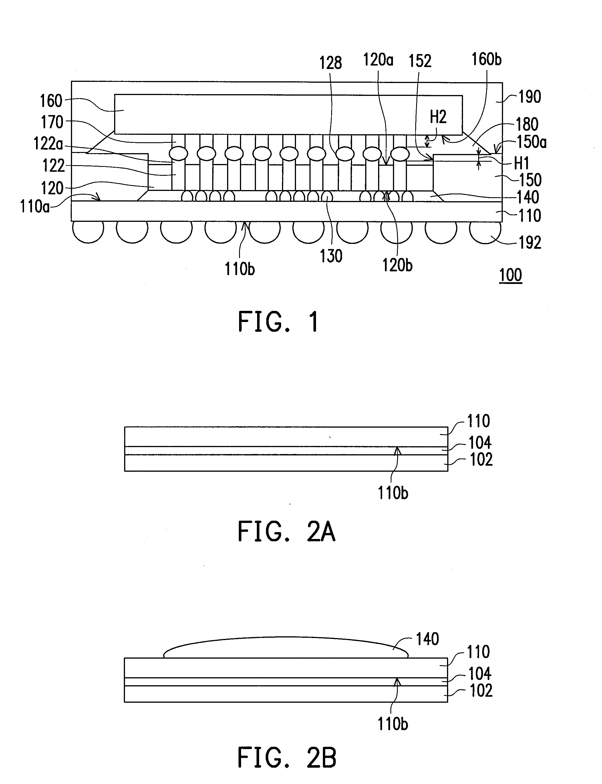
[0042]The present invention uses pillar bumps to connect an upper second chip and a lower first chip so as to control a gap between the first chip and the second chip and overcome a height difference between the first chip and a molding compound surrounding the first chip caused by forming through silicon vias. The aforementioned concept can be applied to various stacked semiconductor device packages, and some package structures and package processes of stacked semiconductor device package are illustrated in the following embodiments.

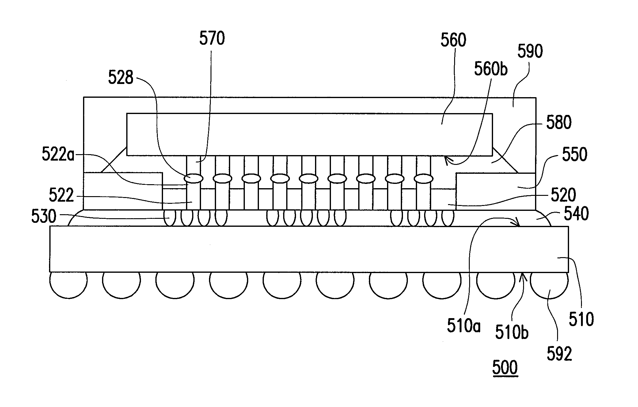
[0043]FIG. 1 illustrates a package structure according to an embodiment of the present invention. As shown in FIG. 1, the package structure 100 of the present embodiment comprises a circuit substrate 110, a first chip 120, a plurality of first bumps 130, a first underfill 140, a first molding compound 150, a second chip 160, a plurality of pillar bumps 170 and a second underfill 180. The circuit substrate 110 has a top surface 110a and a bottom surface ...


PUM


Abstract

A package structure and a package process are proposed in using pillar bumps to connect an upper second chip and through silicon vias of a lower first chip, wherein a gap between the first chip and the second chip can be controlled by adjusting a height of the pillar bumps. In other words, the pillar bumps compensate the height difference between the first chip and a molding compound surrounding the first chip so as to ensure the bondibility between the pillar bumps and the corresponding through silicon vias and improve the process yield. Furthermore, the pillar bumps maintain the gap between the second chip and the molding compound for allowing an underfill being properly filled into the space between the first chip and the second chip.

Description

CROSS-REFERENCE TO RELATED APPLICATION[0001]This is a continuation application of and claims the priority benefit of a prior application Ser. No. 12 / 817,396, filed on Jun. 17, 2010, now pending. The prior application Ser. No. 12 / 817,396 claims the priority benefit of Taiwan patent application serial no. 99116089, filed May 20, 2010. The entirety of each of the above-mentioned patent applications is hereby incorporated by reference herein and made a part of this specification.BACKGROUND OF THE INVENTION[0002]The present invention relates to a package structure and a package process, and particularly relates to a stacked package structure and fabricating process thereof.[0003]In today's information society, users all seek after electronic products with high speed, high quality and multiple functions. In terms of the product exterior appearance, electronic product designs reveal a trend of light weight, thinness and compactness. Therefore, various semiconductor device package technique...

Claims


Application Information

Patent Timeline
Patent Type & Authority Applications(United States)
IPC IPC(8): H01L23/498
CPCH01L21/563H01L21/76898H01L23/3128H01L23/3135H01L2224/83192H01L2225/06548H01L2924/15311H01L2224/73204H01L2224/81191H01L25/0657H01L2224/16148H01L2224/32225H01L2224/32145H01L2224/16227H01L2224/17181H01L2224/92125H01L2224/96H01L2224/16225H01L2924/00H01L2224/16145
Inventor SHEN, CHI-CHIHCHEN, JEN-CHUANCHANG, HUI-SHANCHANG, WEN-HSIUNG
Owner ADVANCED SEMICON ENG INC
Why Eureka
Try Eureka