

Optical Element, Light-Emitting Device, Lighting Device, and Method for Manufacturing Optical Element
a technology of light-emitting elements and optical elements, which is applied in the direction of lighting and heating apparatus, instruments, lenses, etc., can solve the problems of significant light loss and the inability to achieve 100% light extraction efficiency of solid-state light-emitting elements, and achieve the effect of efficient light extraction and high efficiency
- Summary
- Abstract
- Description
- Claims
- Application Information
AI Technical Summary
Benefits of technology
Problems solved by technology
Method used
Image

Examples
embodiment 1
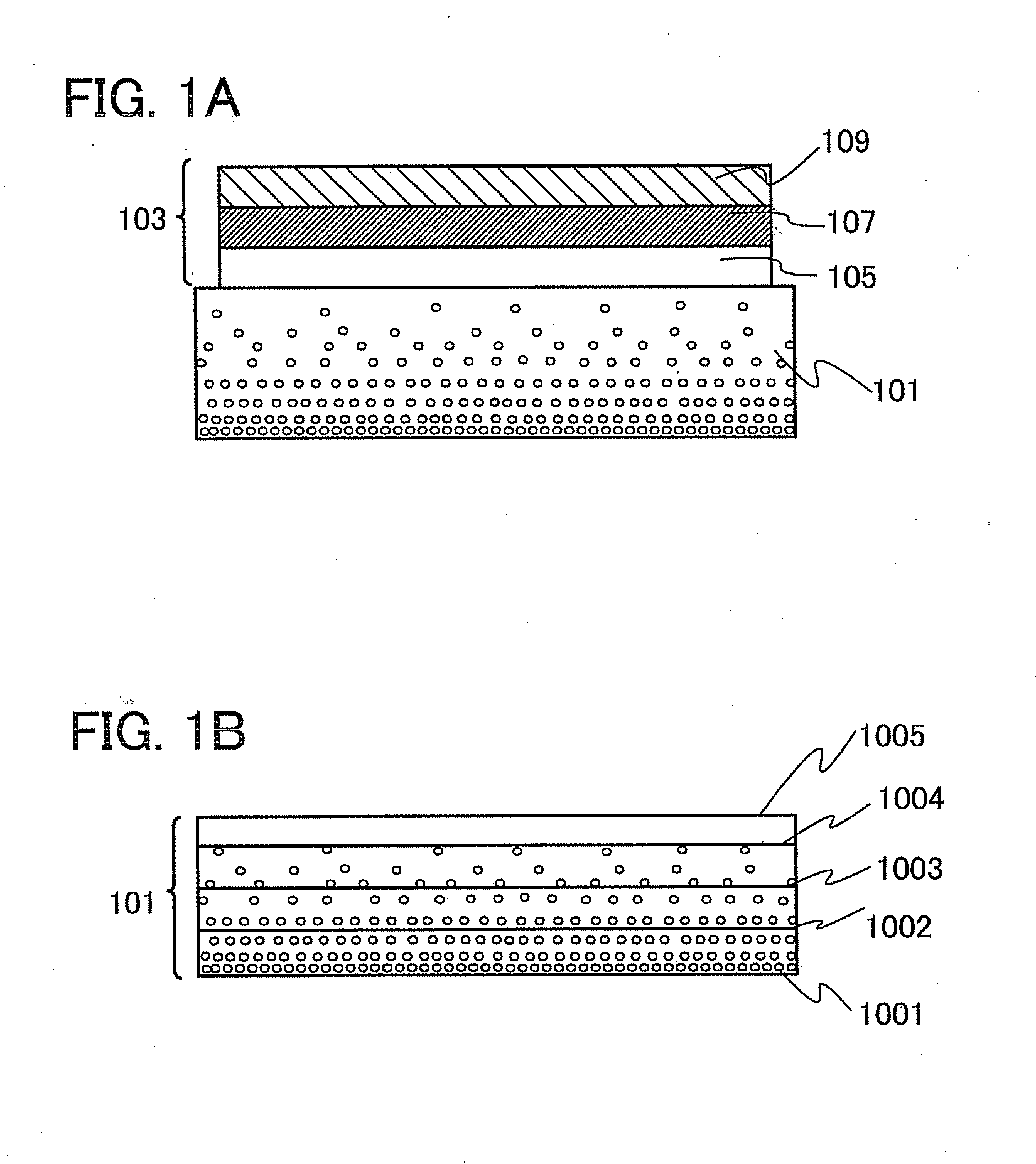
[0040]In this embodiment, an optical element according to one embodiment of the present invention and a light-emitting device including the optical element are described with reference to FIGS. 1A and 1B and FIGS. 2A to 2C.
[0041]As illustrated in FIG. 1A, an optical element 101 has one plane which is in contact with a solid-state light-emitting element 103 and the other plane which is in contact with the air.
[0042]The solid-state light-emitting element 103 includes a transparent electrode 105 which is in contact with the optical element 101, a light-emitting region 107 provided over the transparent electrode 105 and emitting light toward the transparent electrode 105, and a reflective electrode 109 provided over the light-emitting region 107.
[0043]As examples of the solid-state light-emitting element 103, an organic EL element, an inorganic EL element, and an LED can be given. The shape of the solid-state light-emitting element is not particularly limited and may be circular instead...
modification example
[0081]A modification example of the light-emitting device of this embodiment is described.
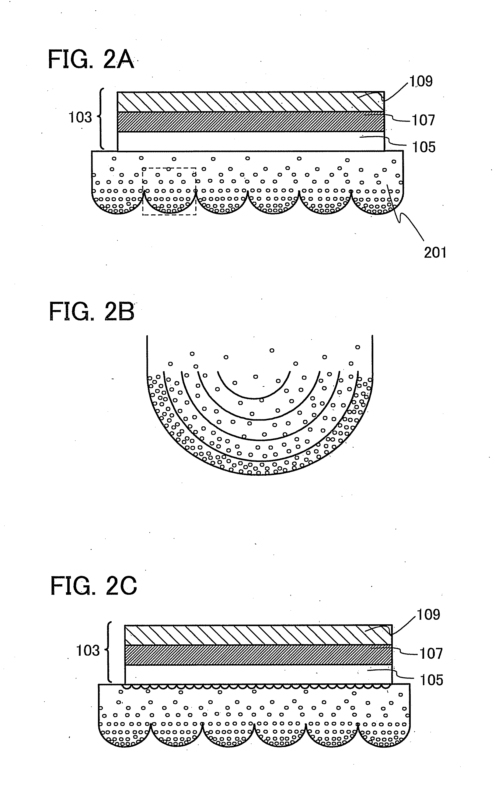
[0082]The optical element of this embodiment may have an uneven structure at the light emission plane.
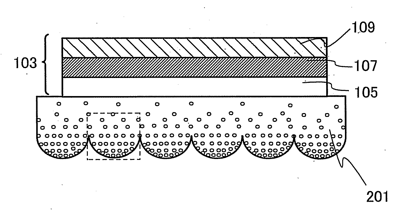
[0083]In FIGS. 2A to 2C, an optical element which has an uneven structure at a light emission plane is illustrated. FIG. 2A is a cross-sectional view, of a light-emitting device whose optical element has a hemispherical structure, and FIG. 2B is an enlarged view of a portion of the hemispherical structure illustrated in FIG. 2A which is surrounded by a dotted line.
[0084]As illustrated in FIG. 2A, in an optical element 201, distribution of bubbles is such that the number density of the bubbles increases from a plane (light incident plane) which is in contact with the solid-state light-emitting element 103 toward a plane (light emission plane) which is in contact with the air, and an apparent refractive index decreases from the light incident plane toward the light emission plane.
[0085]The light ...
embodiment 2
[0108]In this embodiment, a method for manufacturing an optical element according to one embodiment of the present invention is described with reference to FIGS. 3A to 3C and FIGS. 4A to 4C.
[0109]The optical element manufactured by the method described in this embodiment is a flat organic resin member into which bubbles are injected so that an apparent refractive index gradually decreases from one plane toward the other plane.
[0110]In the first step, an organic resin 303 is provided in molds 301 to be shaped as illustrated in FIG. 3A.
[0111]The molds 301 are a pair of molds of an upper mold 301a and a lower mold 301b, which are set between an upper heating plate 305 and a lower heating plate 307 of a heat press. Heat and pressure can be applied to the molds 301 through the upper heating plate 305 and the lower heating plate 307 of the heat press. Further, the upper heating plate 305 and the lower heating plate 307 are supplied with heat by respective heat sources, so that the upper m...
PUM
| Property | Measurement | Unit |
|---|---|---|
| Diameter | aaaaa | aaaaa |
| Diameter | aaaaa | aaaaa |
| Temperature | aaaaa | aaaaa |
Abstract
Description
Claims
Application Information