Light-emitting device and method for manufacturing the same

a technology of light-emitting devices and manufacturing methods, which is applied in the direction of semiconductor/solid-state device manufacturing, semiconductor devices, electrical devices, etc., can solve the problems of led module and system deterioration, led module and module performance degradation, etc., to increase the amount of extracted light, widen the area, and reduce the effect of heat dissipation

Inactive Publication Date: 2015-01-08
PANASONIC INTELLECTUAL PROPERTY MANAGEMENT CO LTD
View PDF22 Cites 5 Cited by
  • Summary
  • Abstract
  • Description
  • Claims
  • Application Information

AI Technical Summary

Benefits of technology

[0026]In accordance with the light-emitting device of the present invention, the both performances of “heat releasing” and “light extraction” can be suitably achieved (see FIG. 1). Specifically, “surface contact between the light-emitting element and the light-emitting element electrode part” can result in a wider area occupied by the light-emitting element electrode part in the light-emitting element, which leads to a suitable achievement of the high heat-releasing performance. Furthermore, there is provided such a structure that the light-emitting element is positioned over the light-emitting element electrode part, i.e., a face-down structure where the electrode of the light-emitting element faces downward. This means that such an inconvenience that “electrode / bump on the upper side of the light-emitting element blocks light” can be avoided, which can increase the amount of the extracted light from the device.
[0027]With respect to the “heat-releasing performance” according to the present invention, a mounting with a bump is not provided (that is, there is provided a mounting-less / bump-less device), which enables the heat from the light-emitting element to be released effectively via the area of “surface contact of the light-emitting element and the electrode part”. In this regard, the light-emitting element electrode part can be made of a material with high thermal conductivity (e.g., copper material), and also can be provided as “electrode part with its large thickness” and / or “electrode part with its large size in a width direction thereof”. Therefore, the present invention makes it possible to effectively release the heat via the electrode part to the outside thereof. It should be noted that the reflective layer itself is made of a suitable material (e.g., metal material) which at least exhibits the thermal conductivity, and also is provided in a very thin form, and thus the thermal resistance of the reflective layer is negligibly small.
[0028]With respect to the “light extraction performance”, the face-down structure according to the present invention makes it possible not only to extract the light effectively from the upper surface of the light-emitting device, but also to extract the light effectively from the lower surface of the light-emitting device due to the presence of the reflective layer. In this regard, the “reflective layer with high reflectivity” is provided directly under the light-emitting element, and thus the light emitted downward from the light-emitting element can be effectively reflected by the reflective layer, which leads to an effective utilization of the downward-emitted light. That is, the light-emitting device of the present invention has a desirable structure for extracting the light not only from the upper surface of the device but also from the lower surface of the device.
[0029]Furthermore, the light-emitting device of the present invention has a “substrate-less structure”. In this regard, the electrode part serves as the supporting layer for supporting the light-emitting element in the light-emitting device of the present invention. The substrate-less structure can lead to the downsizing of the device and also contributes to the low cost of the manufacturing. As such, the device of the present invention can have a suitable flexibility, compared to the conventional device with the high heat-releasing substrate (e.g., ceramic substrate) being used therein as a supporting part.
[0030]The device of the present invention also has such a suitable structure that is capable of wiring directly from the light-emitting element and also achieving a form of array, thereby providing a higher degree of design freedom. Moreover, the device of the present invention has a satisfactory stability of the connection due to the “mounting-less / bump-less”.
[0031]When focusing on the manufacturing method of the present invention, the method has such more simplified processes that the electrode part is directly formed on the light-emitting element and the electrode foundation layer used for the direct formation of the electrode part is eventually used as the reflective layer of the light-emitting device. The simplified manufacturing processes can provide the light-emitting device which is capable of satisfying the both performances of “heat releasing” and “light extraction”. Also, the foundation layer in itself can contribute to the formation of the light-emitting element electrode part (in particular, the formation of the electrode part having a large thickness), while being eventually used as the “reflective layer contributing to the light extraction”. This means that the formation of the foundation layer contributes to not only the improved process, but also the improved final product. In addition, the manufacturing method of the present invention provides a variety of advantageous effects. For example, there is provided such an effect that the redistribution of the wiring can be applied directly to the light-emitting element (e.g., a LED chip), an effect that a wafer-sized chip can be positioned arbitrarily, and an effect that the LED can be sealed on a carrier layer (and thus a light-emitting surface can be smooth), and the like.

Problems solved by technology

The increased current applied to the LED, however, can be a severe operating condition for the LED, causing the performance of the LED to be degraded.
The degradation of the LED inhibits the long lifetime and high reliability in the LED package and module.
Accordingly, the temperature tends to rise in the LED module for lighting and a system thereof, which leads to a deterioration of the LED module and the system.

Method used


Image

  • Light-emitting device and method for manufacturing the same
  • Light-emitting device and method for manufacturing the same
  • Light-emitting device and method for manufacturing the same

Examples


process embodiment 1

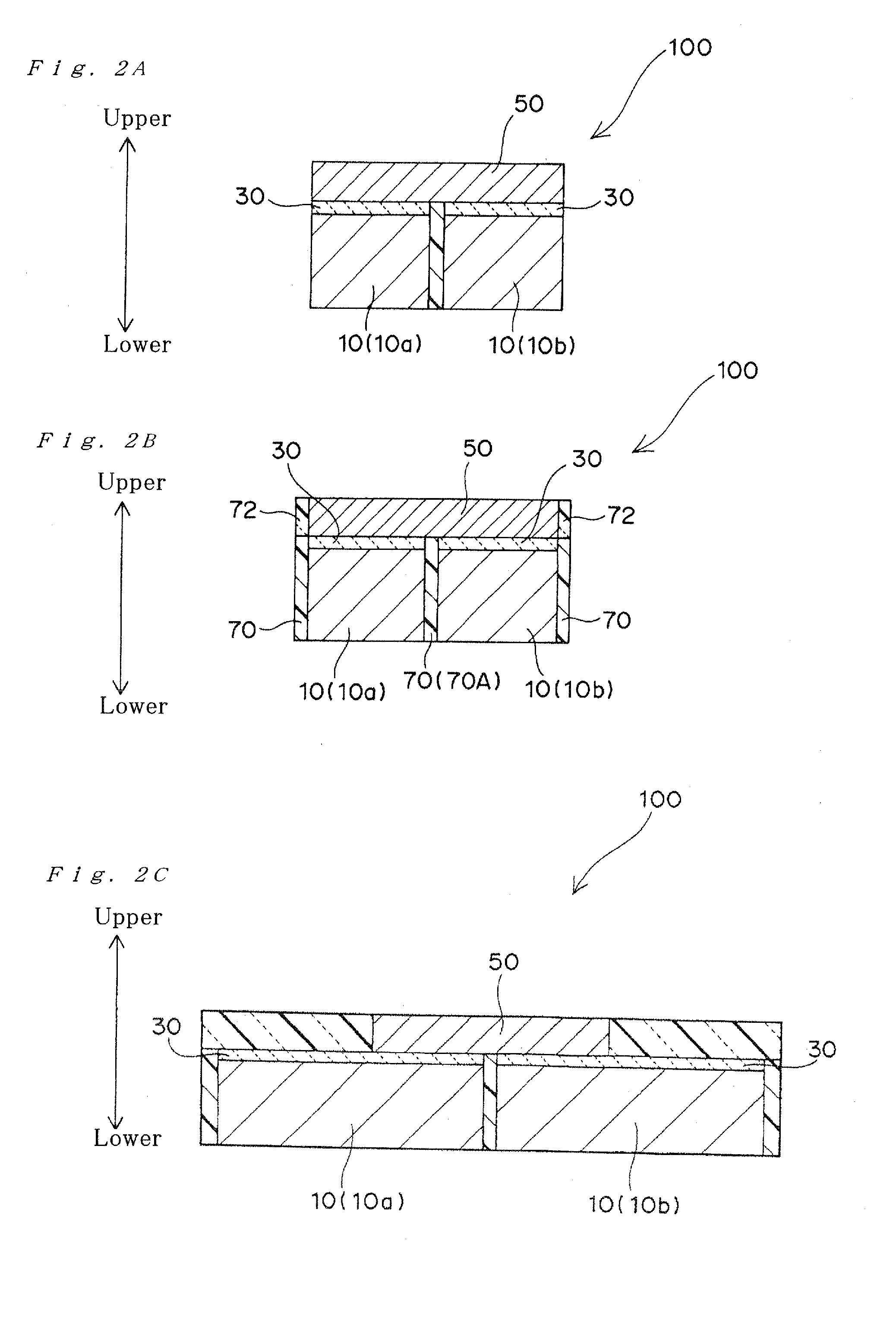
[0088]FIGS. 12A-12G illustrate schematic sectional views of the processes according to “Process Embodiment 1”. This embodiment corresponds to the processes for carrying out the manufacturing of the light-emitting device, based on a LED wafer. Firstly, as shown in FIGS. 12A and 12B, a sealing layer 72′ is formed on a principal surface of a LED wafer 50′. The sealing layer 72′ may be formed by applying a raw material onto the principal surface of the LED wafer by a doctor blade process or a spin coating process, followed by a heat treatment thereof. Alternatively, the sealing layer 72′ may also be formed by superimposing a sealing film onto the LED wafer. Then, as shown in FIG. 12C, electrode foundation layer 30 is formed, for example, by a dry plating process (e.g., sputtering process). Then, as shown in FIG. 12D, a sub-electrode part pattern 10′ is formed directly on the LED wafer 50 via the electrode foundation layer 30. The formation of the sub-electrode part pattern 10′ may be pe...

process embodiment 2

[0093]FIGS. 16A-16H illustrate schematic sectional views of the processes according to “Process Embodiment 2”. This embodiment corresponds to the processes for carrying out the manufacturing of the light-emitting device, based on LED chips. Firstly, as shown in FIG. 16A, a plurality of LED chips 50 are disposed on a carrier film 85 with being spaced away from each other. Then, as shown in FIG. 16B, a sealing layer 72′ (in particular, a light-permeability sealing layer) is formed on the carrier film 85, and thereby the LED chips 50 are covered with the sealing layer. Subsequent to the formation of the sealing layer 72′, the career film 85 is removed, and thereby obtaining the LED chips 50 buried in the sealing layer 72′ as shown in FIG. 16C. That is, there can be provided the light-emitting elements with the sealing layer being located at least on the principal surfaces of the light-emitting elements. In particular, the light-emitting elements 50 buried in the sealing layer 72′ is pr...

process embodiment 3

[0097]FIGS. 17A-17G illustrate schematic sectional views of the processes according to “Process Embodiment 3”. This embodiment corresponds to a modification of “Process Embodiment 2”. Firstly, as shown in FIG. 17A, a plurality of LED chips 50 are disposed on a carrier film 85 with being spaced away from each other. Then, an insulating film 72′ (e.g., insulating film made of inorganic material) is formed between the neighboring LED chips 50. As illustrated, the insulating film 72′ is preferably formed such that it is flush with the LED chips 50. The patterning of the insulating layer 72′ can be performed in the above-described manner with respect to “Process Embodiment 1” (see FIGS. 15A(a)-15A(c) or 15B). Subsequent to the patterning of the insulating layer 72′, a phosphor layer 80 is formed on the LED chips 50 and the insulating layer pattern 72′ (see FIG. 17B), and thereafter the carrier film 85 is removed. As a result, there can be provided the light-emitting elements 50 as shown ...


PUM


Abstract

There is provided a light-emitting device comprising a light-emitting element. The light-emitting device of the present invention comprises an electrode part for the light-emitting element; a reflective layer provided on the electrode part; and the light-emitting element provided on the reflective layer such that the light-emitting element is in contact with at least a part of the reflective layer, wherein the light-emitting element and the electrode part are in an electrical connection with each other by mutual surface contact via the at least a part of the reflective layer, wherein the electrode part serves as a supporting layer for supporting the light-emitting element, and wherein the electrode part extends toward the outside of the light-emitting element and beyond the light-emitting element.

Description

TECHNICAL FIELD[0001]The present invention relates to a light-emitting device and a method for manufacturing the light-emitting device. More particularly, the present invention relates to a light-emitting device equipped with a light-emitting diode (which is referred to also as “LED” hereinafter) and a method for manufacturing such device.BACKGROUND OF THE INVENTION[0002]In recent years, a LED has been used in various applications because it is considered as being energy-saving light source and having a long lifetime. For example, the LED is used as backlight source for display device (e.g., liquid crystal display). Furthermore the LED is used in camera flash applications and automotive applications, and also in various lighting applications. The high brightness of the LED is generally achieved by an increase in an applied current to the LED, i.e., by an increase in the amount of light. The increased current applied to the LED, however, can be a severe operating condition for the LE...

Claims


Application Information

Patent Timeline
Patent Type & Authority Applications(United States)
IPC IPC(8): H01L33/38H01L33/60H01L33/50
CPCH01L33/38H01L33/507H01L33/60H01L2933/0058H01L2933/0025H01L2933/0041H01L2933/0016H01L24/17H01L33/486H01L33/62H01L2933/0033H01L33/64H01L2224/16225H01L2224/49107H01L2224/48091H01L2224/45144H01L2924/12041H01L2924/00014H01L2924/00H01L2924/15747H01L2924/15787H01L33/647H01L2924/12042H01L33/505H01L2933/0066
Inventor SAWADA, SUSUMUNAKATANI, SEIICHIKAWAKITA, KOJIYAMASHITA, YOSHIHISA
Owner PANASONIC INTELLECTUAL PROPERTY MANAGEMENT CO LTD
Why Eureka
Try Eureka