Three-dimensional memory array stacking structure

a memory array and stacking technology, applied in the field of memory devices, can solve the problems of complex manufacturing process with a high cost per bit, high parasitic wiring resistance, and significant engineering challenges in the design and fabrication of three-dimensional memory arrays

Active Publication Date: 2012-08-23
RAMBUS INC
View PDF16 Cites 167 Cited by
  • Summary
  • Abstract
  • Description
  • Claims
  • Application Information

AI Technical Summary

Problems solved by technology

The design and fabrication of three-dimensional memory arrays present significant engineering challenges.
For example, architectures for three-dimensional resistance-switching random access memory (RRAM) may require numerous photolithograph

Method used


Image

  • Three-dimensional memory array stacking structure
  • Three-dimensional memory array stacking structure
  • Three-dimensional memory array stacking structure

Examples


Embodiment Construction

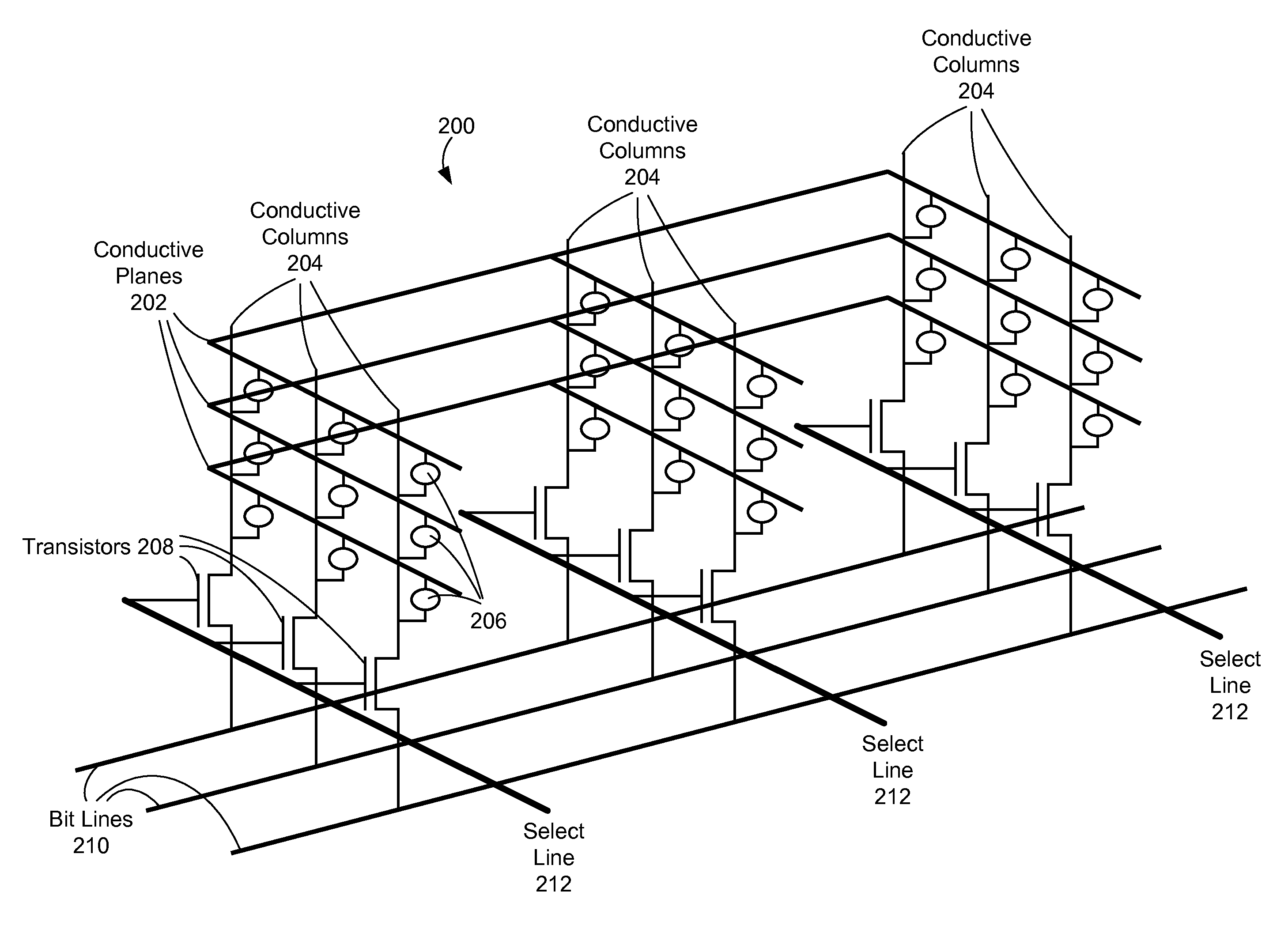
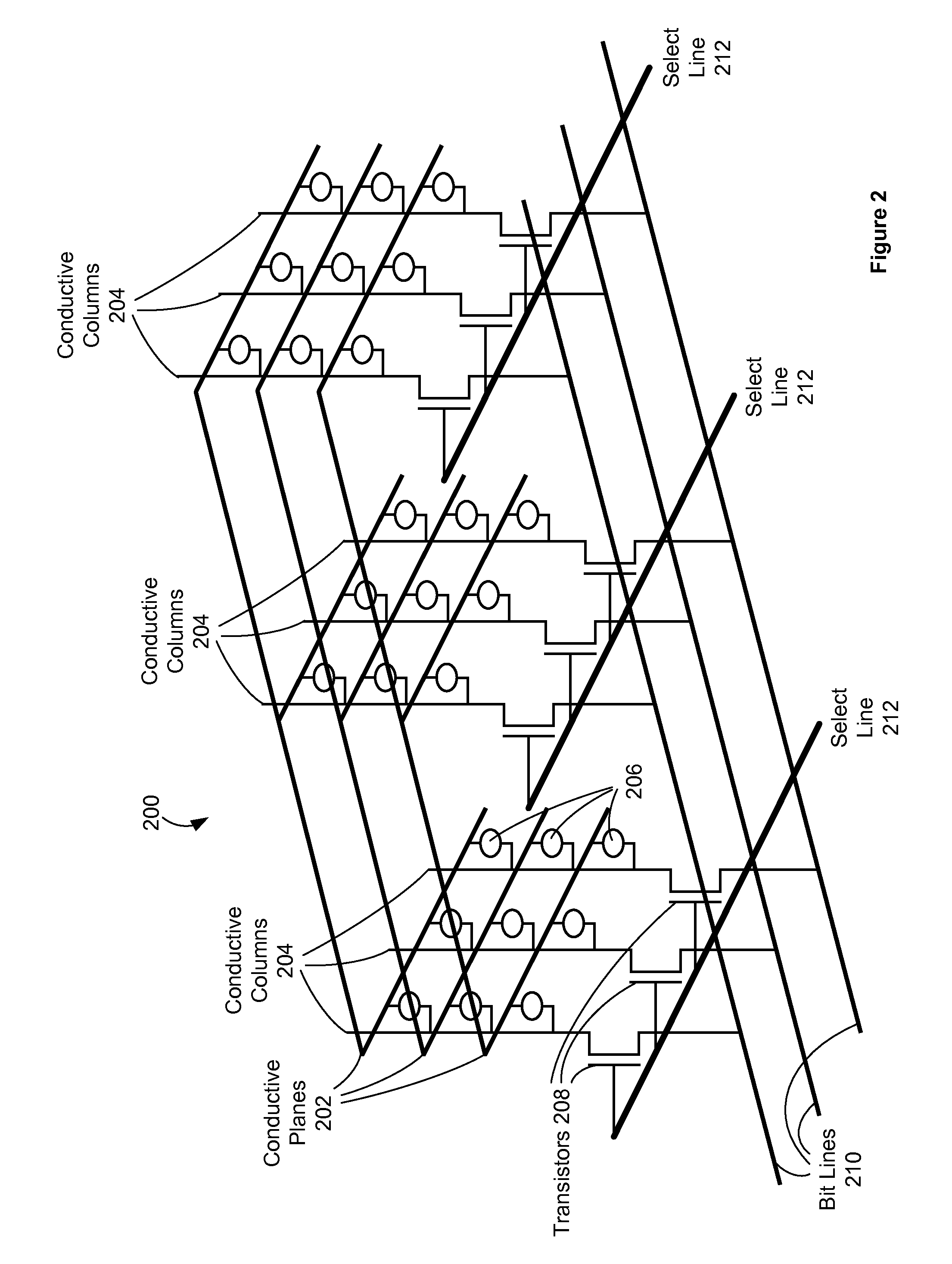
[0023]A memory device has a three-dimensional array stacking structure. The structure includes a planar substrate, a plurality of horizontal conductive planes above the planar substrate, and a plurality of horizontal insulating layers interleaved with the plurality of horizontal conductive planes. Vertical conductive columns, perpendicular to the conductive planes and insulating layers, pass through apertures in the conductive planes and insulating layers. Finally, each memory element of the memory device couples one of the horizontal conductive planes to a respective vertical conductive column.

[0024]To program or store information in this memory device, a horizontal conductive plane and a vertical conductive column are selected, and then a voltage is applied between the selected horizontal conductive plane and the selected vertical conductive column to program the programmable memory element that couples the selected horizontal conductive plane to the selected vertical conductive c...


PUM


Abstract

A memory device includes a planar substrate, a plurality of horizontal conductive planes above the planar substrate, and a plurality of horizontal insulating layers interleaved with the plurality of horizontal conductive planes. An array of vertical conductive columns, perpendicular to the pluralities of conductive planes and insulating layers, passes through apertures in the pluralities of conductive planes and insulating layers. The memory device includes a plurality of programmable memory elements, each of which couples one of the horizontal conductive planes to a respective vertical conductive column.

Description

TECHNICAL FIELD[0001]The disclosed embodiments relate generally to memory devices, and more particularly, to three-dimensional memory architectures.BACKGROUND[0002]The design and fabrication of three-dimensional memory arrays present significant engineering challenges. For example, architectures for three-dimensional resistance-switching random access memory (RRAM) may require numerous photolithographic processing steps to fabricate the memory array, resulting in a complicated manufacturing process with a high cost per bit. High parasitic wiring resistance also presents challenges in traditional architectures for three-dimensional RRAMs. Accordingly, there is a need for improved three-dimensional memory (e.g., RRAM) architectures.BRIEF DESCRIPTION OF THE DRAWINGS[0003]FIG. 1 shows a plan view of programmable memory elements and associated metal lines in a stacked cross-point array architecture.[0004]FIG. 2 illustrates a schematic diagram of a three-dimensional memory architecture wi...

Claims


Application Information

Patent Timeline
IPC IPC(8): H01L45/00
CPCG11C5/02G11C5/063H01L27/2454H01L27/249H01L45/085H01L45/1266H01L27/2418H01L45/143H01L45/145H01L45/146H01L45/1226H01L27/2409H01L45/142H10B63/22H10B63/34H10B63/845H10B63/20H10N70/245H10N70/823H10N70/8416H10N70/8822H10N70/8825H10N70/883H10N70/8833H10B63/80
Inventor KELLAM, MARK D.BRONNER, GARY B.
Owner RAMBUS INC
Why Eureka
Try Eureka