Interposer, packages including the interposer, and methods

a technology of interposer and interposer, which is applied in the field of interposer, packages including the interposer, and methods, can solve the problem that the interposer opening may not extend a sufficient lateral distance, and achieve the effect of facilitating the connection

Inactive Publication Date: 2002-11-14
MICRON TECH INC
View PDF8 Cites 89 Cited by
  • Summary
  • Abstract
  • Description
  • Claims
  • Application Information

AI Technical Summary

Problems solved by technology

Consequently, in order to maintain the structural integrity of chip-scale package interposers, the interposer openings may not extend a sufficient lateral distance beyond bond pads of their corresponding semiconductor devices to provide adequate clearance for the tip of a wire bonding capillary or other intermediate conductive element-forming, -positioning, or securing apparatus to properly access the bond pads.

Method used


Image

  • Interposer, packages including the interposer, and methods
  • Interposer, packages including the interposer, and methods
  • Interposer, packages including the interposer, and methods

Examples


Embodiment Construction

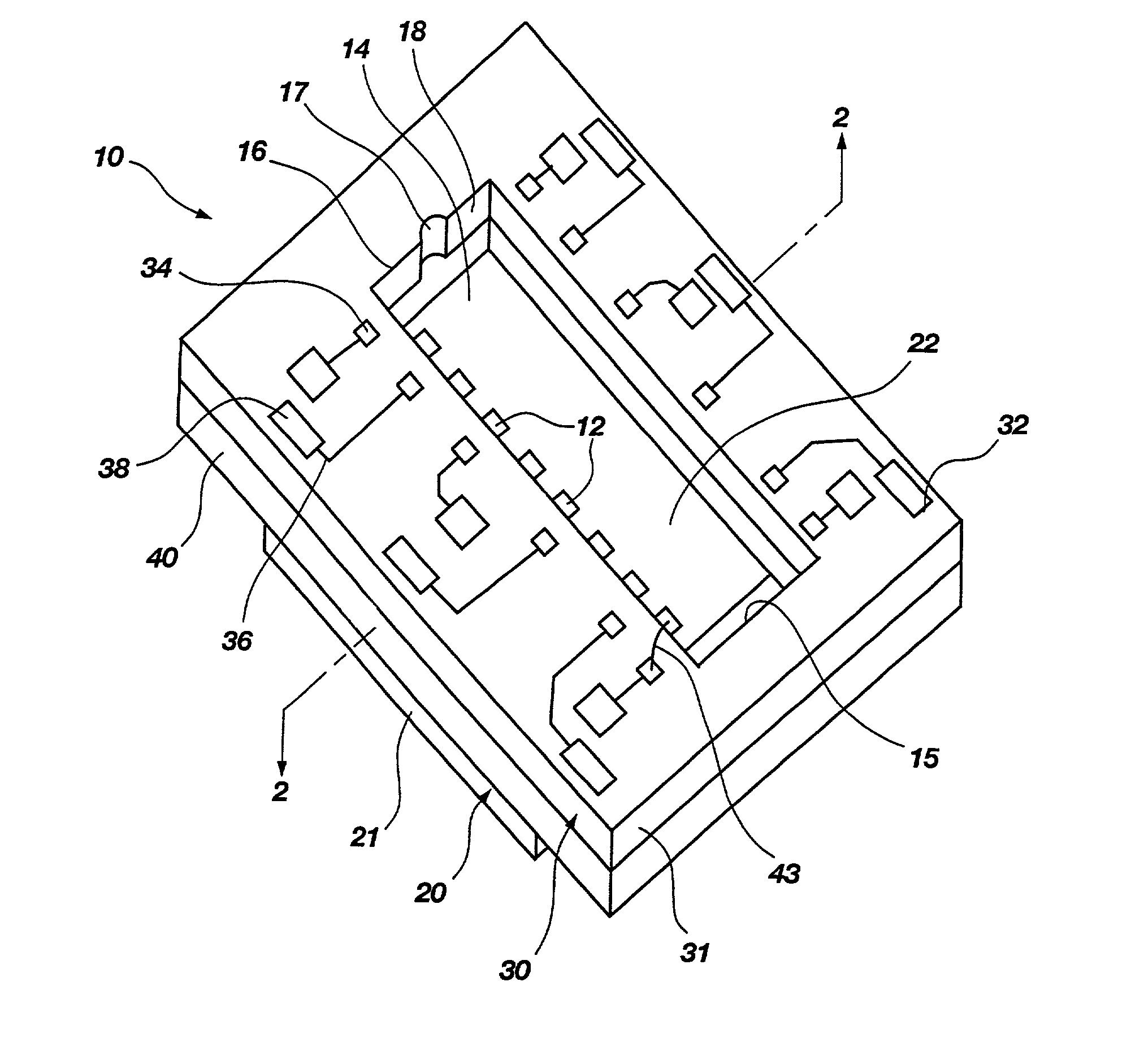
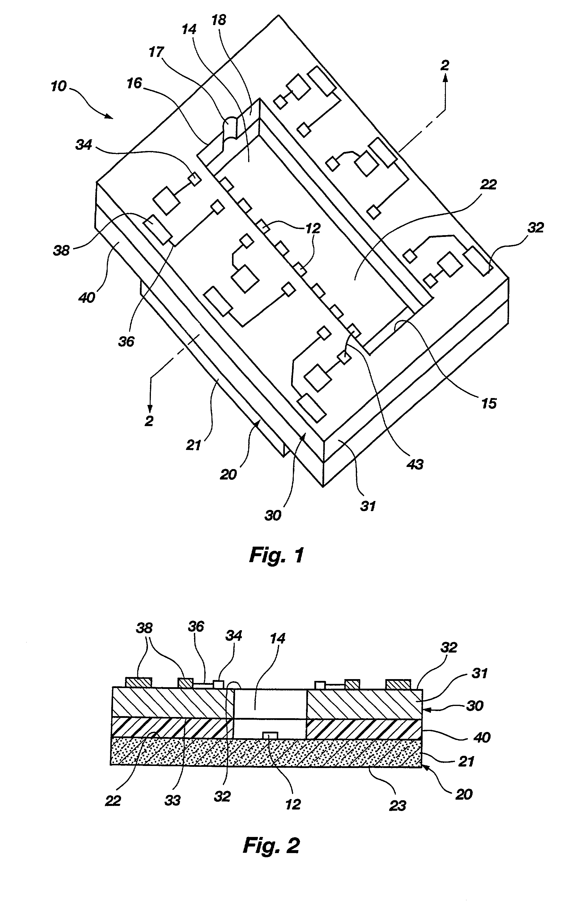
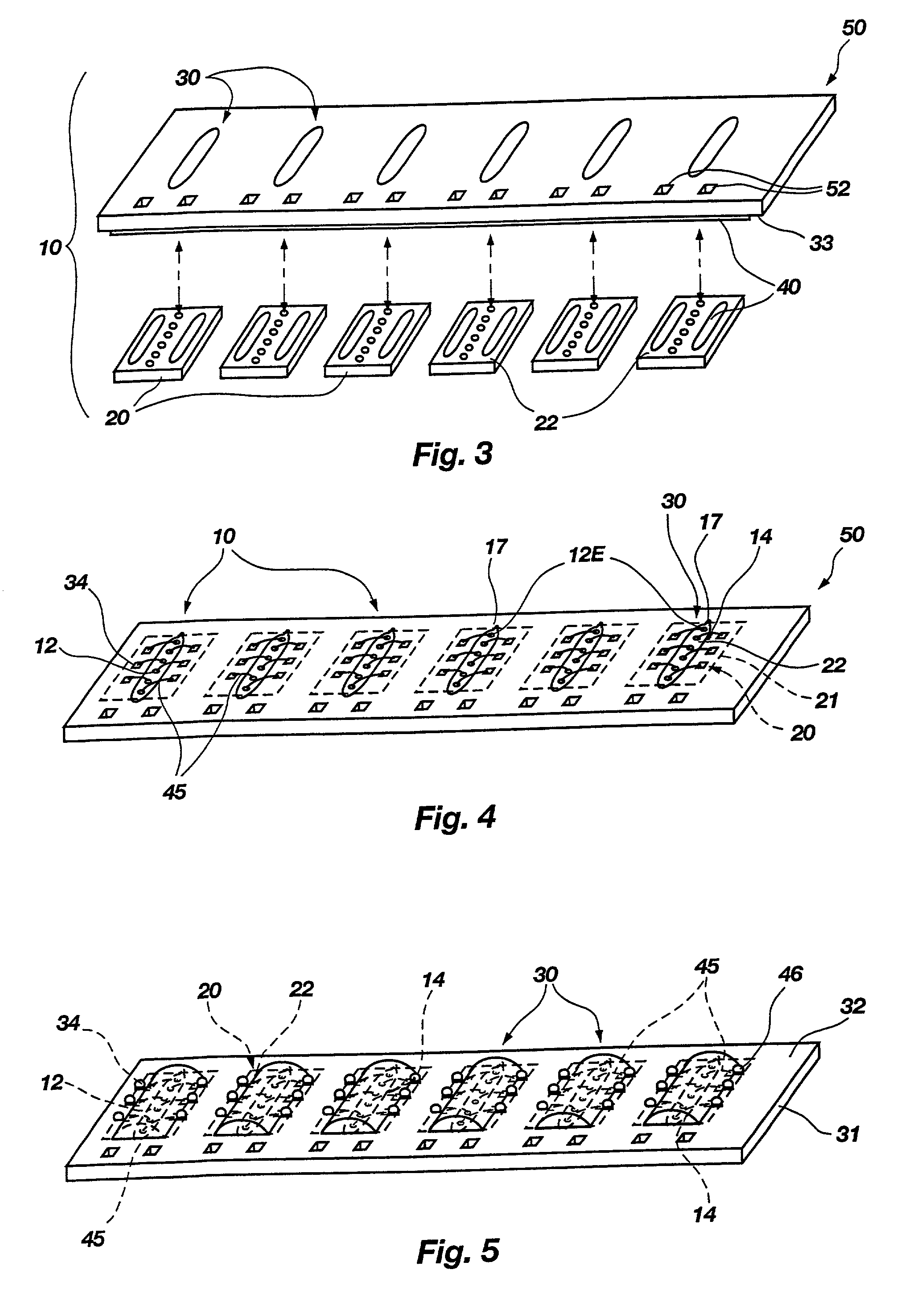
[0027] Although it has many applications in semiconductor die packaging, an interposer or another substrate element of the present invention may best be described in relation to a board-on-chip assembly 10. A semiconductor device assembly 10 incorporating teachings of the present invention, as shown in FIGS. 1 and 2, has conductive structures 46 (e.g. balls, bumps, or pillars of solder, another metal or metal alloy, or z-axis conductive elastomer) protruding therefrom in a ball grid array connection pattern and includes a semiconductor die 20 and a substrate element, which is also referred to herein as an interposer 30.

[0028] The interposer 30 includes a substantially planar substrate element 31 that may be formed from any suitable material, such as resin (e.g., FR-4 resin), plastic, insulator-coated semiconductor material (e.g., silicon oxide-coated silicon), glass, ceramic, or any other suitable, electrically insulative or at least partially dielectric-coated material, may be posi...


PUM

PropertyMeasurementUnit
areaaaaaaaaaaa
electricallyaaaaaaaaaa
conductiveaaaaaaaaaa

Abstract

An interposer including a substantially planar substrate element with a slot formed therethrough. The slot, through which bond pads of a semiconductor die are exposed upon assembly of the interposer with the semiconductor die, includes a laterally recessed area formed in only a portion of a periphery thereof. The laterally recessed area is positioned so as to expose at least a portion of an active surface of the semiconductor die located between a bond pad located adjacent an outer periphery of the semiconductor die and the outer periphery. The laterally recessed area facilitates access to the bond pad by apparatus for forming, positioning, or securing intermediate conductive elements. Semiconductor device assemblies and packages that include the interposer are also disclosed, as are methods for assembling semiconductor device components with the interposer and methods for packaging such assemblies.

Description

[0001] The present invention relates generally to interposers for use in semiconductor device packages and, more specifically, to interposers that are to be assembled with semiconductor dice having bond pads arranged substantially linearly across central regions of the active surfaces thereof. In particular, the present invention relates to interposers including slots formed therethrough that are configured to facilitate the connection of bond wires to bond pads that are located proximate the edges of semiconductor dice to be assembled with the interposers. The present invention also relates to ball grid array packages including the interposers, as well as to methods for assembling the interposers with semiconductor devices and methods for forming ball grid array packages that include the interposers.[0002] The dimensions of many different types of state of the art electronic devices are ever decreasing. To reduce the dimensions of electronic devices, the structures by which the mic...

Claims


Application Information

Patent Timeline
Patent Type & Authority Applications(United States)
IPC IPC(8): H01L21/48H01L23/13H01L23/498H05K3/00
CPCH01L21/4803Y10T408/03H01L23/49811H01L24/45H01L24/48H01L24/50H01L24/97H01L2224/45124H01L2224/45144H01L2224/4824H01L2224/73215H01L2224/97H01L2924/01013H01L2924/01014H01L2924/01079H01L2924/09701H05K3/0044H05K2203/0228H05K2203/1476H01L23/13H01L2924/01087H01L2924/01033H01L2924/01006H01L2924/01005H01L2924/00014H01L2224/85H01L24/86H01L2924/12042H01L2924/181H01L2924/00
Inventor FEE, SETHO SINGYEAN, TAY WUUCHYE, LIM THIAM
Owner MICRON TECH INC
Why Eureka
Try Eureka