Thermal detector, thermal detection device, and electronic instrument

a thermal detection and detector technology, applied in the direction of optical radiation measurement, semiconductor devices, instruments, etc., can solve the problems of difficult to reduce element size and increase detail, and the effect of infrared light absorbing film is not high, and it is difficult to completely cancel out the interaction between the first reflected infrared light and the second reflected infrared ligh

Active Publication Date: 2012-08-23
SEIKO EPSON CORP
View PDF9 Cites 21 Cited by
  • Summary
  • Abstract
  • Description
  • Claims
  • Application Information

AI Technical Summary

Benefits of technology

[0109]A number of embodiments were described above, but as will be readily appreciated by a person skilled in the art, numerous modifications can be made provided that they do not deviate substantially from the novel matter and effect of the invention. Consequently, examples of such modifications are included within the scope of the invention. For example, in the specification or drawings, in at least one instance, terms that are presented along with different terms that have a broader meaning or the same meaning may be replaced with these different terms in some locations.
[0110]The present invention is not restricted to the embodiments described above; various modifications and improvements may be included. Modification examples are described below.Modification

Problems solved by technology

In Japanese Laid-Open Patent Application Publication No. 2000-205944, the respective energy intensities of the first reflected infrared light that is reflected by the infrared light absorbing film and the second reflected light that is reflected by the completely reflective film are different, and so it is not possible to completely cancel out interactions between the first reflected infrared light and the second reflected infrared light.
As a result, there is the problem that the effective absorption at the infrared light absorbing film is not high.
For this reason, there is the problem that it is difficult to reduce element size and to increase detail when arranging elements in a two-dimensional array.

Method used


Image

  • Thermal detector, thermal detection device, and electronic instrument
  • Thermal detector, thermal detection device, and electronic instrument
  • Thermal detector, thermal detection device, and electronic instrument

Examples


embodiment 1

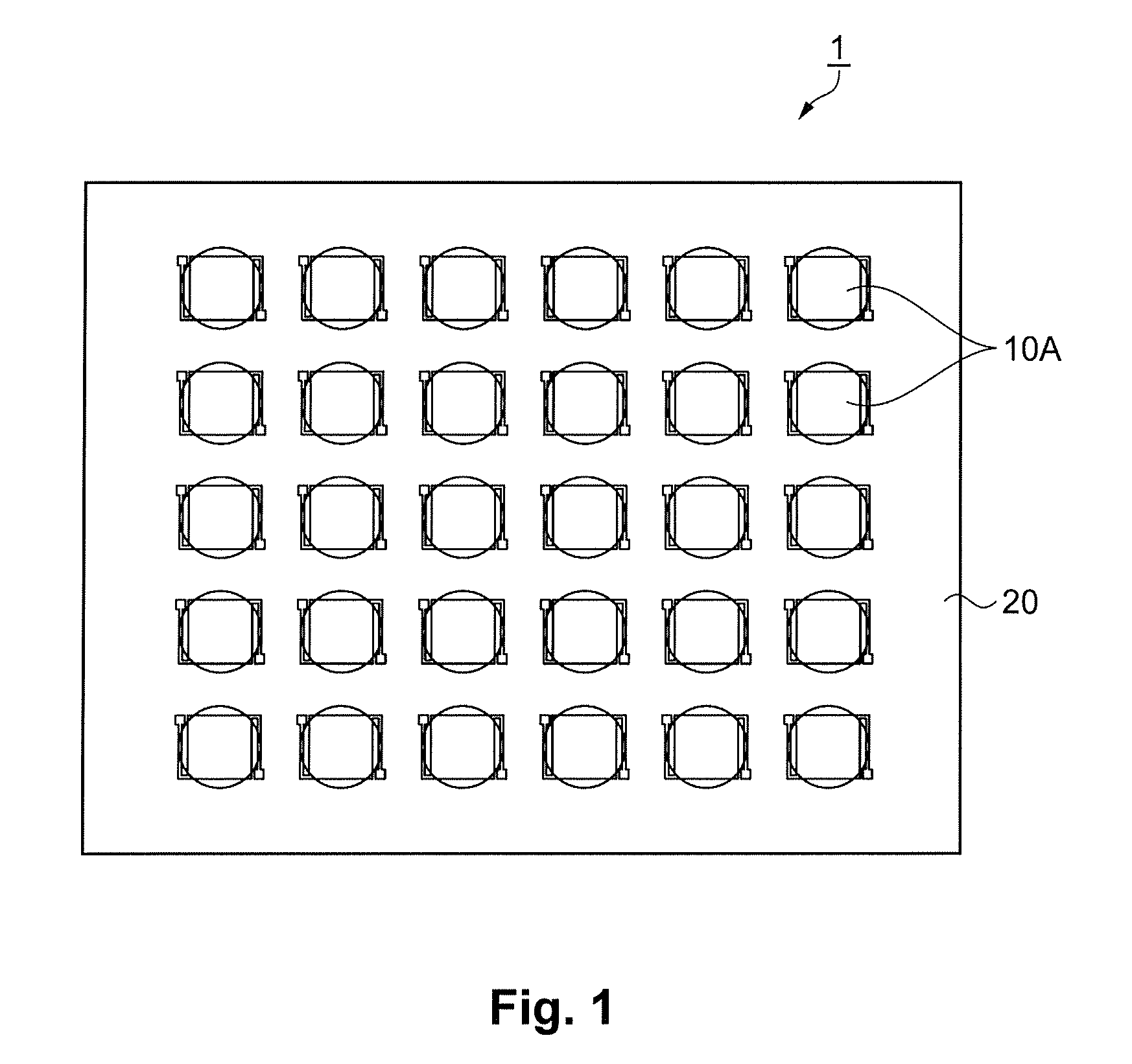
[0038]FIG. 1 is a schematic plan view showing an infrared detection device. As shown in FIG. 1, the infrared light detection device 1 has a substrate 20. Thermal detectors 10A are disposed as individual cells in a two-dimensional grid-shaped matrix on the substrate 20. Each cell denotes the section in which a thermal detector 10A has been disposed. The thermal detectors 10A detect infrared light and thus the infrared detection device 1 can detect an infrared light distribution. The infrared detection device 1 can thus provide a thermal (light) distribution image.

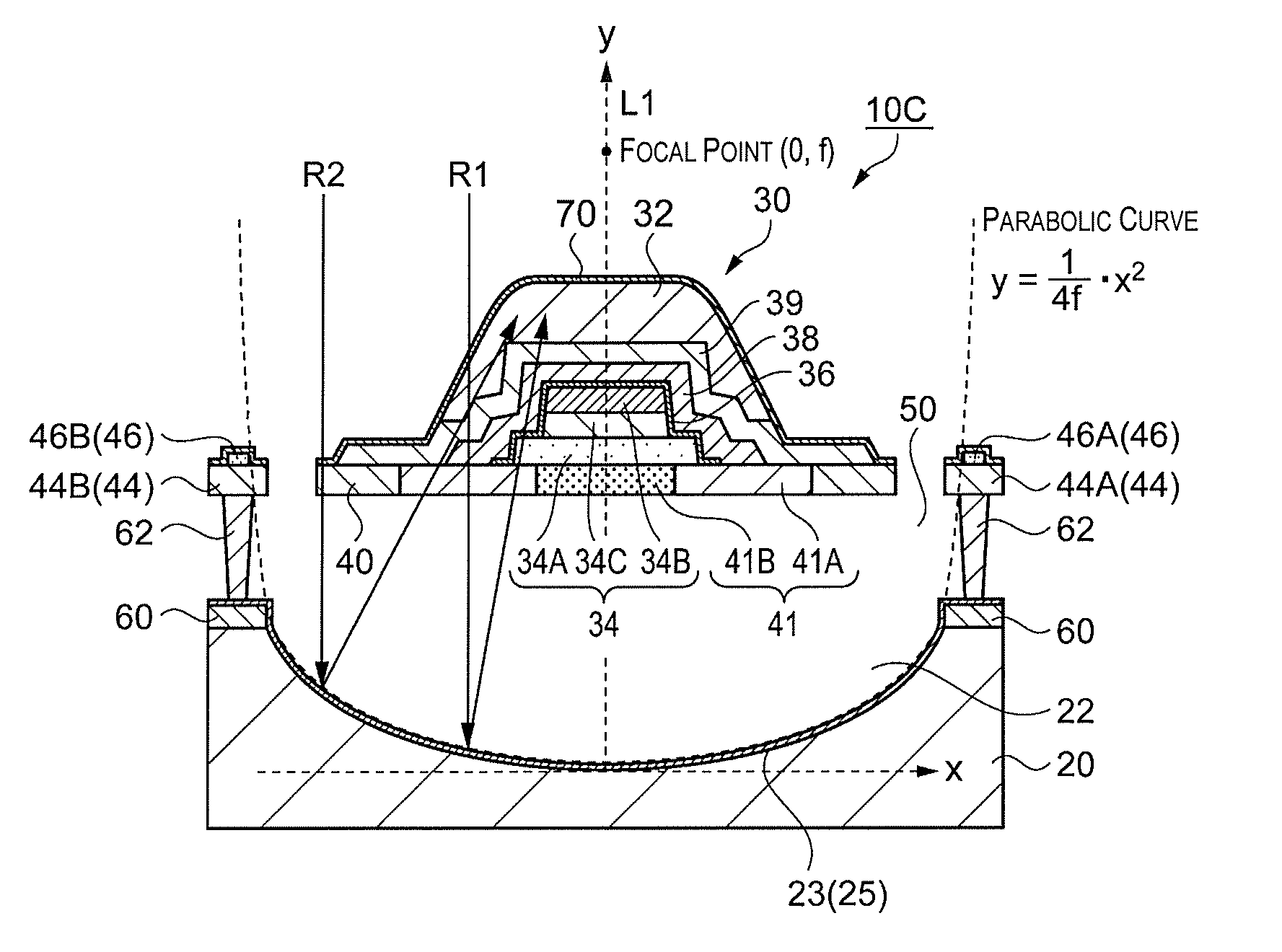
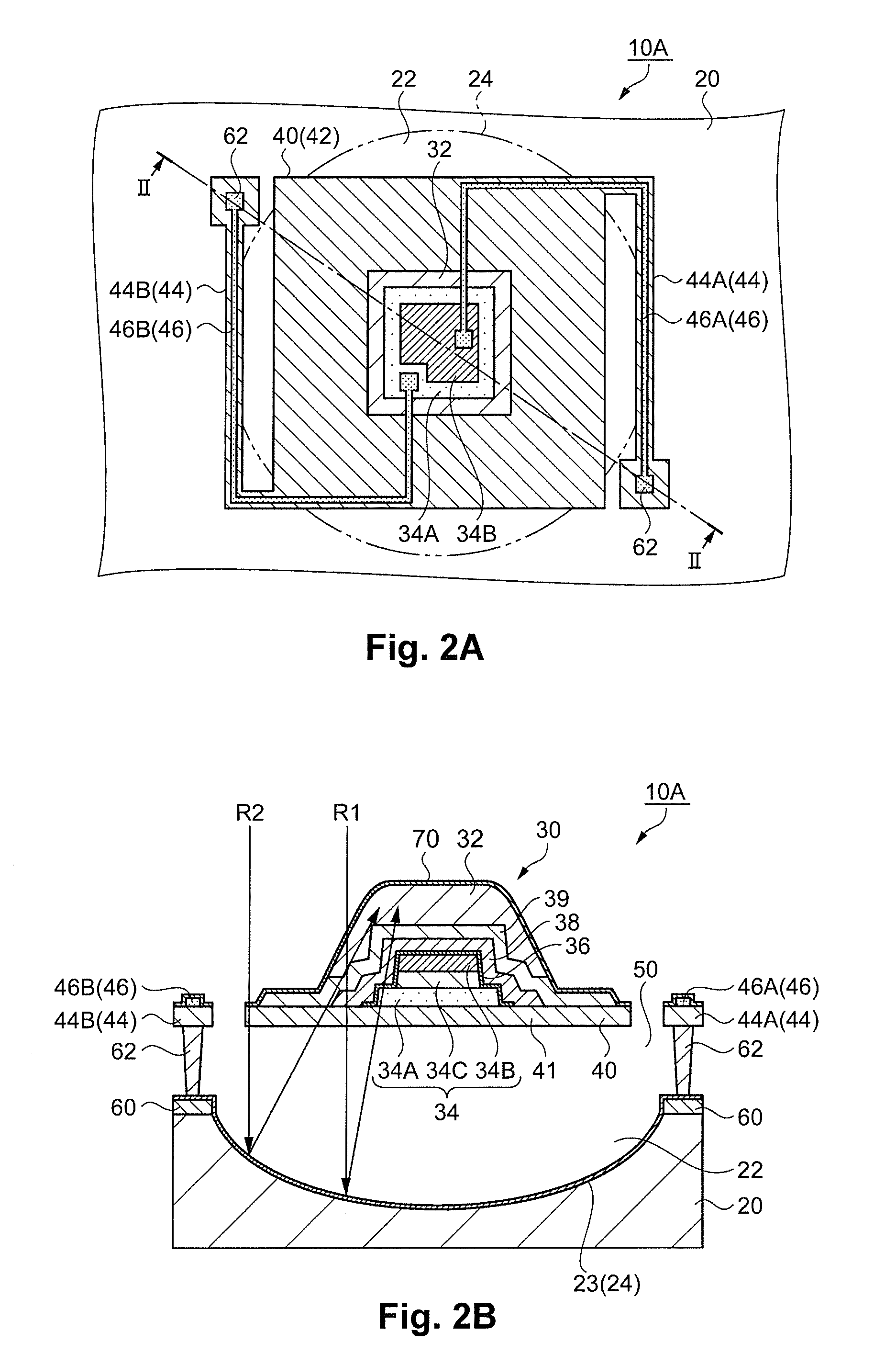
[0039]FIG. 2A is a schematic plan view that shows an infrared detector. FIG. 2B is a schematic sectional view of the infrared detector taken along the line II-II in FIG. 2A. First, the general configuration will be described for the thermal detector 10A that is used as the infrared detector in Embodiment 1.

[0040]As shown in FIGS. 2A and 2B, the thermal detector 10A has a second recess part 22 that is used as the recess part,...

embodiment 2

[0079]A characteristic thermal detector according to a second embodiment is described below using FIGS. 5 and 6. In this embodiment, the same designations are used for similar members or regions as in Embodiment 1, and detailed descriptions are not provided.

[0080]With this embodiment, in contrast to Embodiment 1, the light-absorbing part 41 has doped regions in which impurities have been dispersed into polycrystalline silicon and undoped regions that contain no impurities.

[0081]FIG. 5A is a schematic plan view of the thermal detector as viewed from the support member 40 towards the substrate 20. FIG. 5B is a schematic sectional view of the thermal detector sectioned along line III-III in FIG. 5A. The thermal detector 10B shows a single cell. First, the general structure of the thermal detector 10B that serves as the infrared detector will be described.

[0082]As shown in FIG. 5, the doped regions 41A and the undoped regions 41B in the light-absorbing part 41 are in a patterned layout....

embodiment 3

[0093]Next, a characteristic thermal detector according to Embodiment 3 will be described with reference to FIGS. 7 to 10. In this embodiment, the same designations are used for similar members or regions as in Embodiment 1, and detailed descriptions are not provided.

[0094]This embodiment differs from Embodiment 1 insofar as the shape of the curved light-reflecting surface 24 is different.

[0095]FIG. 7 is a schematic sectional view showing the infrared detector, and FIG. 8 is a diagram detailing a parabolic surface. In FIG. 7, the bottom surface 23 of the second recess part 22 in the thermal detector 10C is a parabolic surface, not a spherical surface. As shown in FIG. 8A, given a reference line L2 (y=−f) that is parallel to the X axis and perpendicular to the Y axis and a focal point F (y=f) on the Y-axis, the parabolic curve that forms the parabolic surface is given as the locus of points P for which points Q exist on the reference line L2 such that the distance PQ is equivalent to...


PUM


Abstract

A thermal detector includes a substrate, a thermal detection element and a support member. The substrate has a recess part with a bottom surface of the recess part being a curved light-reflecting surface. The thermal detection element has a light-absorbing film. The support member supports the thermal detection element. The substrate and the support member are arranged to form a hollow part therebetween. The support member includes a light-absorbing part in which impurities are dispersed in polycrystalline silicon with the light-absorbing part being arranged in at least a part of a surface of the support member facing toward the hollow part so that the light-absorbing part being irradiated by light.

Description

CROSS-REFERENCE TO RELATED APPLICATIONS[0001]This application claims priority to Japanese Patent Application No. 2011-036817 filed on Feb. 23, 2011. The entire disclosure of Japanese Patent Application No. 2011-036817 is hereby incorporated herein by reference.BACKGROUND[0002]1. Technical Field[0003]The present invention relates to a thermal detector, a thermal detection device, and an electronic instrument.[0004]2. Related Art[0005]Pyroelectric-type and bolometer-type infrared light detection devices are known thermal detection devices. Infrared light detection devices detect infrared light based on the heat that is produced when an infrared light-absorbing film absorbs infrared light, causing an excitation voltage to be produced in the detection element (pyroelectric-type) or causing a resistance value to change (bolometer-type).[0006]In order to improve sensitivity by increasing infrared light absorption, it has been proposed that the diaphragm that constitutes the infrared light...

Claims


Application Information

Patent Timeline
Patent Type & Authority Applications(United States)
IPC IPC(8): H01L31/101
CPCH01L37/02H01L31/0547Y02E10/52H01L31/101G01J5/0806G01J5/023G01J5/10G01J5/20G01J5/34G01J5/0853H10N15/10
Inventor TSUCHIYA, YASUSHI
Owner SEIKO EPSON CORP
Why Eureka
Try Eureka