Mask for screen printing, screen printing device and screen printing method employing same

a technology of screen printing and printing device, which is applied in the direction of foil printing, coating, inking apparatus, etc., can solve the problems of printing failure, thin film circuit board, and flexible printed circuit board on which electronic components are mounted low production cost, and achieve high printing quality. , the effect of preventing printing failur

Inactive Publication Date: 2012-08-30
PANASONIC CORP
View PDF3 Cites 4 Cited by
  • Summary
  • Abstract
  • Description
  • Claims
  • Application Information

AI Technical Summary

Benefits of technology

[0012]According to the present invention, a recess is formed so as to correspond to the array of the circuit boards on the lower surface of the flat mask plate of the mask. Having a flat part, the recess is capable of accommodate at least one of the circuit boards. A pattern hole is formed only in the recess. The structure above allows the carrier to have a flat holding surface with a simple structure, preventing printing failure. As a result, a plurality of circuit boards held by the carrier undergoes printing operation with high printing quality at a low cost.

Problems solved by technology

A thin film circuit board, such as a flexible printed circuit board on which electronic components are mounted, has difficulty in handling.
The methods above, however, have some problems in achieving high printing quality and low production cost.
In the area with a clearance caused by poor contact, the paste cannot be properly printed on the surface so that the phenomenon causes printing failure.
These necessities have increased cost of preparing a carrier with recesses, and accordingly, hampered reduction of production cost.
As described above, for printing the paste for connecting electronic components simultaneously on circuit boards held by a carrier, a conventional screen printing device has difficulty in achieving high printing quality at a low cost.

Method used


Image

  • Mask for screen printing, screen printing device and screen printing method employing same
  • Mask for screen printing, screen printing device and screen printing method employing same
  • Mask for screen printing, screen printing device and screen printing method employing same

Examples


Embodiment Construction

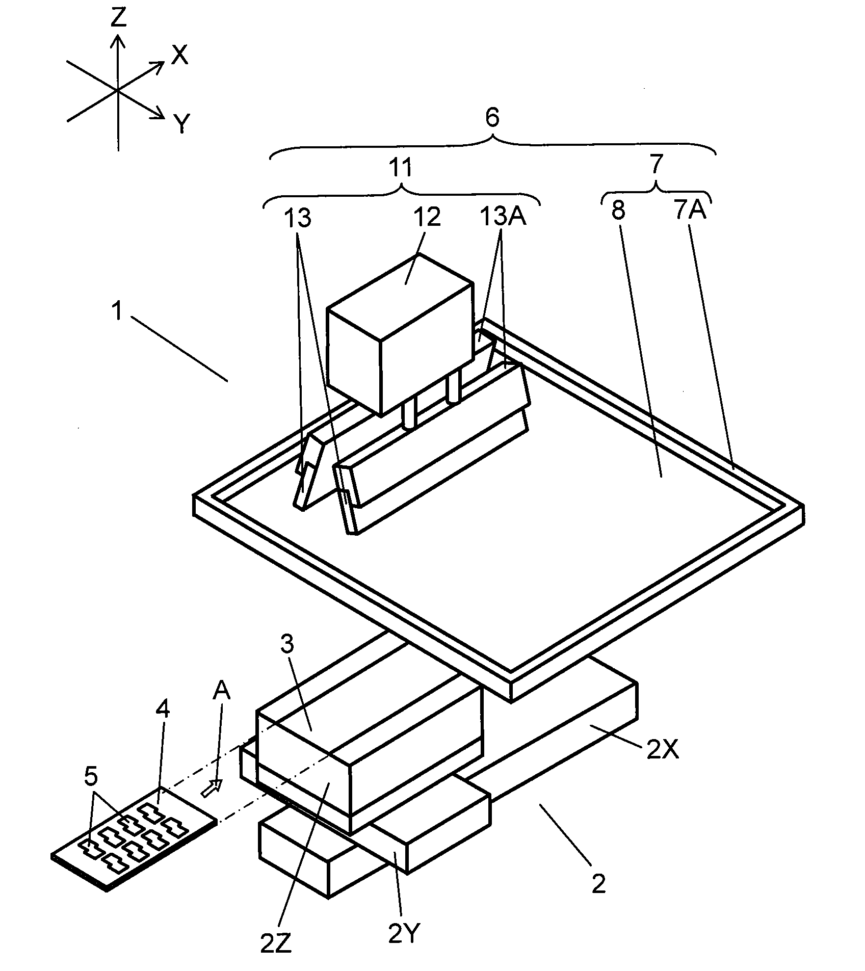
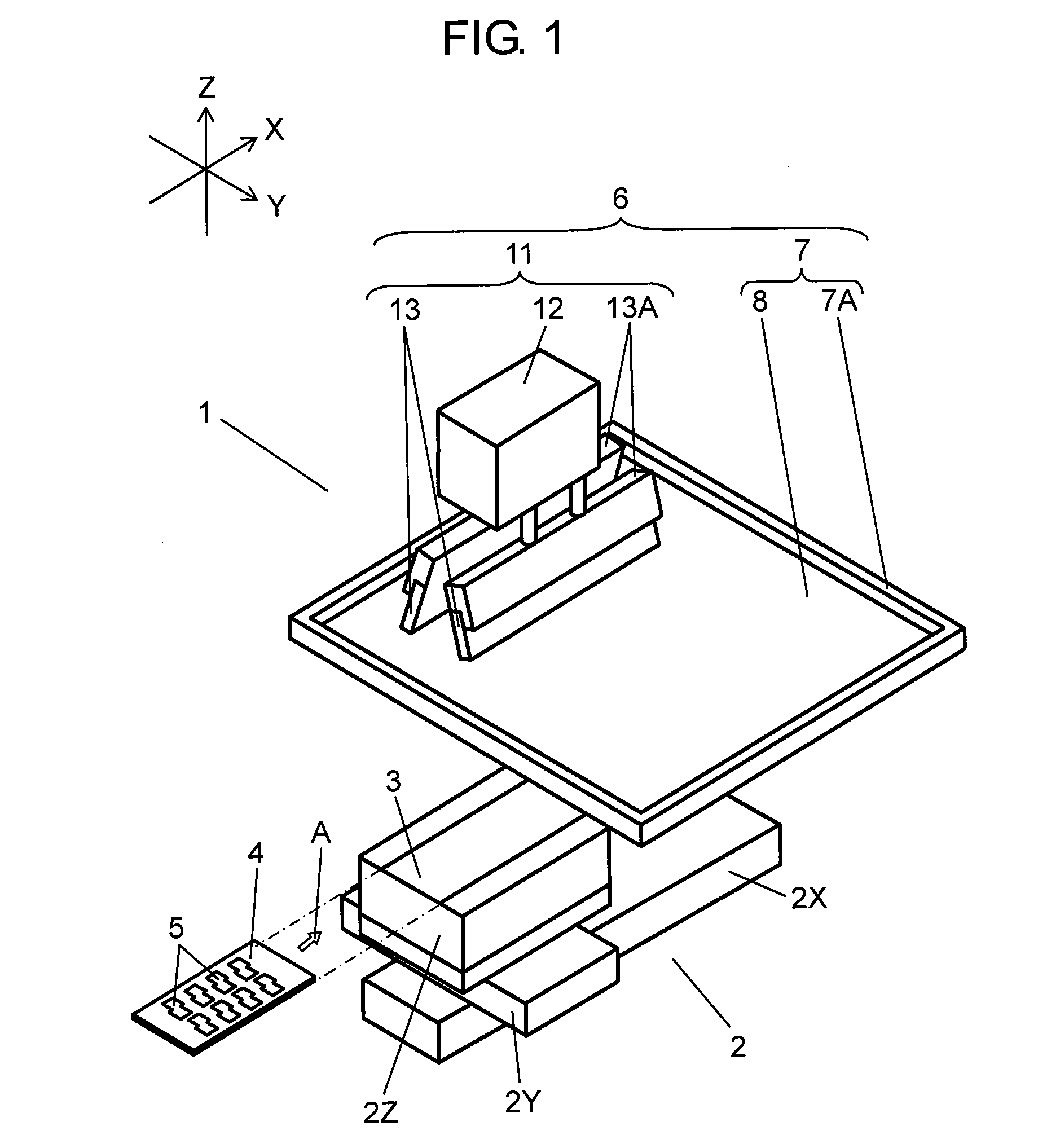
[0032]FIG. 1 is a perspective view showing a screen printing device in accordance with an exemplary embodiment of the present invention. FIG. 2 is a perspective view showing a carrier used with the screen printing device shown in FIG. 1. FIG. 3 is a plan view of the carrier shown in FIG. 2. FIG. 4 is a perspective plan view of a mask for screen printing used for the screen printing device shown in FIG. 1. FIGS. 5A through 5D illustrate the printing operation by the screen printing device shown in FIG. 1.

[0033]First, the structure of screen printing device 1 is described with reference to FIG. 1 and FIG. 3. Circuit boards 5 are fixed on or held by carrier 4. Screen printing device 1 prints paste, which is to be used for connecting electronic components to circuit board 5, simultaneously on electrode 51 formed on each of circuit boards 5.

[0034]Screen printing device 1 has printing mechanism6 including screen printing mask 7 disposed over carrier positioning section 2. That is, screen ...


PUM


Abstract

The screen printing mask is used for printing paste simultaneously on circuit boards held by the carrier. The mask has a flat mask plate. On the lower surface of the mask plate, a flat-bottomed recess capable to accommodating at least one of the circuit boards is formed so as to correspond to the array of the circuit boards on the carrier. A pattern hole is formed only in the recess.

Description

TECHNICAL FIELD[0001]The present invention relates to a screen printing mask used in printing paste for connecting electronic components onto circuit boards held by a carrier. The present invention also relates to a screen printing device and a screen printing method employing the mask.BACKGROUND ART[0002]A thin film circuit board, such as a flexible printed circuit board on which electronic components are mounted, has difficulty in handling. For easy handling, such a circuit board is handled in a manner that circuit boards are fixed on or are held by a plate-like carrier. That is, while being held by a carrier, the circuit boards undergo printing of paste for connecting electronic components and component mounting work (for example, see patent literatures 1 through 4).[0003]In the examples of patent literatures 1 and 2, the carrier has an adhesive surface formed of silicone elastomer or the like so that the circuit boards are held by the adhesion of the surface. In the examples of ...

Claims


Application Information

Patent Timeline
Patent Type & Authority Applications(United States)
IPC IPC(8): B05C17/06
CPCB41F15/0881B41F15/36B41N1/248B41F15/46H05K3/007H05K3/0097H05K3/1225B41P2215/50
Inventor TOMOMATSU, MICHINORIIKEDA, MASANORITANIGUCHI, MASAHIROFURUICHI, SATOSHI
Owner PANASONIC CORP
Why Eureka
Try Eureka