Pixel circuit and display device

a display device and pixel circuit technology, applied in the field of pixel circuits and display devices, can solve the problems of deterioration of display quality, insufficient contrast, and decrease of average potential in each frame period, and achieve the effect of improving display quality and improving contras

Inactive Publication Date: 2012-08-30
SHARP KK
View PDF11 Cites 6 Cited by
  • Summary
  • Abstract
  • Description
  • Claims
  • Application Information

AI Technical Summary

Benefits of technology

[0018]The present invention has been made in consideration of the above problems and, it is an object of the present invention to provide a pixel circuit and a display device that can prevent deterioration of a liquid crystal and display quality with a low power consumption without causing a decrease in aperture ratio. In particular, it is an object to provide a pixel circuit and a display device in which, also when a pixel circuit is configured on an amorphous silicon substrate having a small mobility, the pixel voltage obtained after writing can be maintained without influencing the pixel voltage.
[0111]When a plurality of pixel circuits are arranged, a normal writing action is generally executed for each row. For this reason, at the maximum, a driver circuit needs to be driven the number of times which is equal to the number of rows of the arranged pixel circuits. In contrast to this, according to the pixel circuit of the present invention, a self-refresh action is performed to make it possible to execute a refresh action to the plurality of arranged pixels at once for each of the held voltage states. For this reason, the number of times of driving of a driver circuit required from the start of the refresh action to the end thereof can be greatly reduced to make it possible to realize a low power consumption. Since a memory unit such as an SRAM need not be additionally arranged in the pixel circuit, an aperture ratio does not decrease unlike in the conventional art.
[0112]In particular, according to the configuration of the present invention, in the self-refresh action, on / off-control of the first transistor element and the third transistor element that configure the second switch circuit can be delayed and executed on purpose. This causes the following effect.

Problems solved by technology

However, when the refresh frequency is lowered, a pixel data voltage held in a pixel electrode varies by a leakage current of a TFT.
Since an average potential in each frame period also decreases, deterioration of display quality such as insufficient contrast may be probably caused.

Method used


Image

  • Pixel circuit and display device
  • Pixel circuit and display device
  • Pixel circuit and display device

Examples


first embodiment

[0166]In the first embodiment, configurations of a display device of the present invention (to be simply referred to as a “display device” hereinafter) and a pixel circuit of the present invention (to be simply referred to as a “pixel circuit” hereinafter) will be described below.

[0167]>

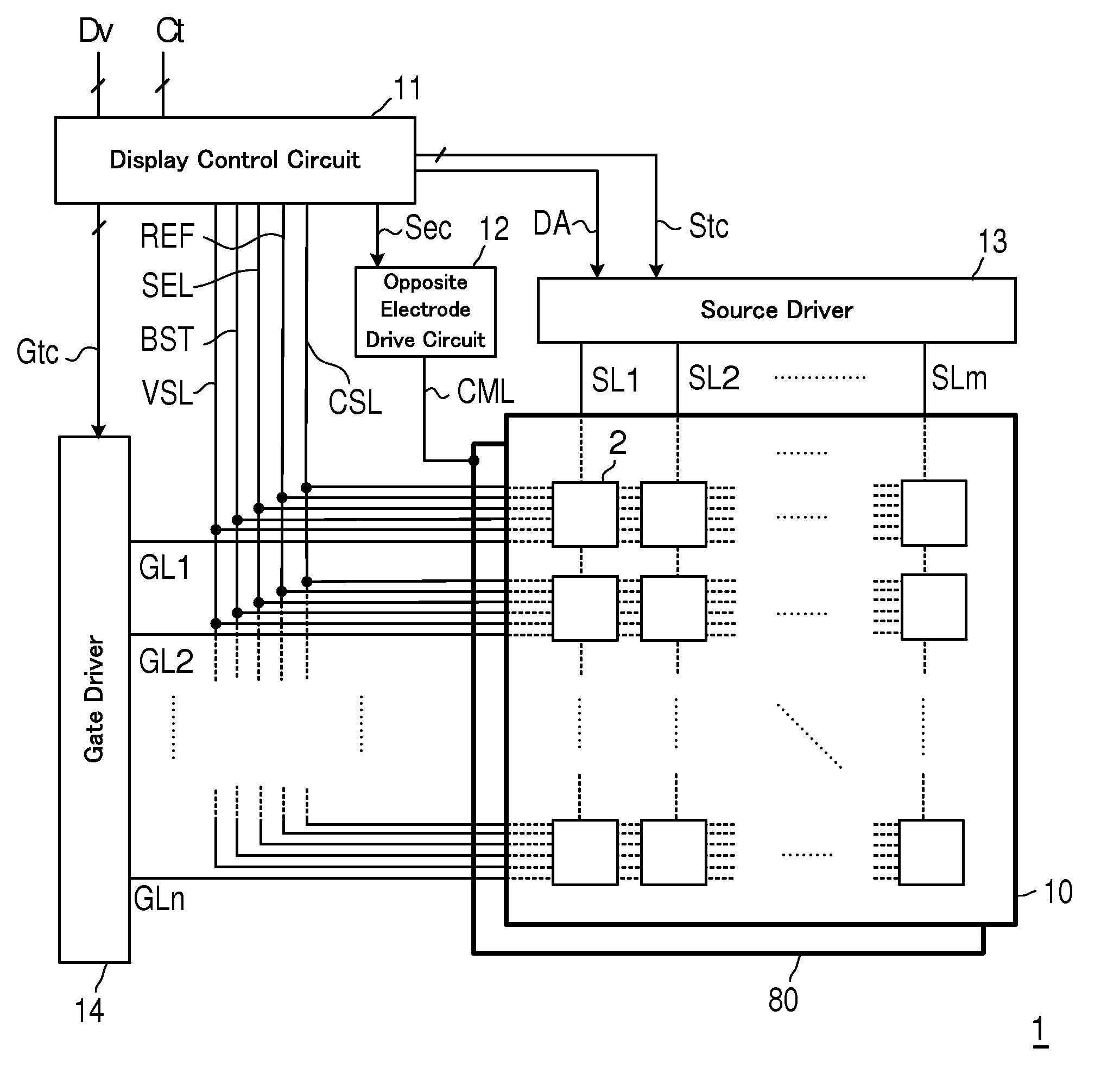
[0168]FIG. 1 shows a schematic configuration of a display device 1. The display device 1 includes an active matrix substrate 10, a counter electrode 80, a display control circuit 11, a counter electrode drive circuit 12, a source driver 13, a gate driver 14, and various signal lines (will be described later). On the active matrix substrate 10, a plurality of pixel circuits 2 are arranged in row and column directions to form a pixel circuit array.

[0169]In FIG. 1, to avoid the drawings from being complex, the pixel circuits 2 are displayed as a block. In order to clarify that the various signal lines are formed on the active matrix substrate 10, for descriptive convenience, the active matrix substrate ...

second embodiment

[0250]In the second embodiment, self-refresh actions performed by the pixel circuits of the first to eighth types of the groups X and Y described above will be described with reference to the accompanying drawings.

[0251]The self-refresh action is an action in an always-on display mode, and is an action in which the first switch circuit 22, the second switch circuit 23, and the control circuit 24 are operated by a predetermined sequence in the plurality of pixel circuits 2 to recover potentials of the pixel electrodes 20 (or potentials of the internal nodes N1) to a potential written by an immediately previous writing action at the same time in a lump. The self-refresh action is an action being unique to the present invention and performed by the pixel circuits. The self-refresh action can achieve a very low power consumption in comparison with an “external refresh action” that performs a normal writing action as in the conventional technique to recover the potential of the pixel ele...

third embodiment

[0356]In a third embodiment, a writing action in an always-on display mode will be described for each of the types with reference to the accompanying drawings.

[0357]In the writing action in the always-on display mode, pixel data of one frame is divided in units of display lines in a horizontal direction (row direction), and a binary voltage corresponding to each pixel data of one display line, i.e., a high-level voltage (5 V) or a low-level voltage (0 V) is applied to the source line SL of each column for each horizontal period. A selected-row voltage of 8 V is applied to the gate line GL of a selected display line (selected row) to turn on the first switch circuits 22 of all the pixel circuits 2 of the selected row, and voltages of the source lines SL of the columns are transferred to the internal node N1 of each of the pixel circuits 2 of the selected row.

[0358]A non-selected row voltage of −5 V is applied to the gate lines GL of display lines (non-selected rows) except for the se...


PUM


Abstract

In a display device including a pixel circuit having a transistor with a low electron mobility, low power consumption is realized without decreasing an aperture ratio. An liquid crystal capacitor element (Clc) is formed between a pixel circuit (20) and a counter electrode (80). One ends of the pixel electrode (20), a first switch circuit (22), and a second switch circuit (23) and a first terminal of a second transistor (T2) form an internal node (N1). The other end of the first switch circuit (22) is connected to a source line (SL). The second switch circuit (23) has the other end connected to a voltage supply line (VSL), and is a series circuit of transistors (T1 and T3). A control terminal of the transistor (T1), a second terminal of the transistor (T2), and one end of the boost capacitor element (Cbst) form an output node (N2). The other end of the boost capacitor element (Cbst) and the control terminal of the transistor (T2) are connected to a selecting line (SEL) and a reference line REF, respectively. A control terminal of the transistor (T3) is connected to the selecting line (SEL) through a delay circuit (31).

Description

REFERENCE TO RELATED APPLICATIONS[0001]This application is a National Phase filing under 35 U.S.C. §371 of International Application No. PCT / JP2010 / 062319 filed on Jul. 22, 2010, and which claims priority to Japanese Patent Application No. 2009-255346 filed on Nov. 6, 2009.FIELD OF THE INVENTION[0002]The present invention relates to a pixel circuit and a display device including the pixel circuit and, in particular, an active-matrix type display device.BACKGROUND OF THE INVENTION[0003]In a mobile terminal such as a cellular phone or a mobile game console, a liquid crystal display device is generally used as a display means. Since a cellular phone is driven by a battery, a power consumption is strongly required to be reduced. For this reason, information such as time or a battery life that is required to be always displayed is displayed on a reflective sub-panel. In recent years, on the same main panel, a normal display by a full-color display and a reflective always-on display have ...

Claims


Application Information

Patent Timeline
Patent Type & Authority Applications(United States)
IPC IPC(8): G09G5/00
CPCG09G3/3614G09G3/3648G09G3/3655G09G3/3659G09G2300/0417G09G2330/021G09G2300/0809G09G2300/0814G09G2300/0876G09G2320/0247G09G2300/0465
Inventor YAMAUCHI, YOSHIMITSU
Owner SHARP KK
Why Eureka
Try Eureka