Liquid crystal display device and manufacturing method therefor

a technology of liquid crystal display and manufacturing method, which is applied in the direction of microlithography exposure apparatus, instruments, photomechanical treatment, etc., can solve the problems of reducing display luminance and response speed distribution, and achieve the effect of suppressing the time and increasing the cost of optical alignment processing

Inactive Publication Date: 2012-09-13
SHARP KK
View PDF0 Cites 14 Cited by
  • Summary
  • Abstract
  • Description
  • Claims
  • Application Information

AI Technical Summary

Benefits of technology

[0050]According to the present invention, in the case where the 4D-RTN mode is adopted for a liquid crystal display device in which one pixel includes a picture element

Problems solved by technology

This causes a problem that there occurs a response speed distribution.
There is another problem that since the li

Method used


Image

  • Liquid crystal display device and manufacturing method therefor
  • Liquid crystal display device and manufacturing method therefor
  • Liquid crystal display device and manufacturing method therefor

Examples


embodiment 1

[0158]Before describing this embodiment, a method for dividing one picture element of a general 4D-RTN mode into domains having different alignment directions, and a problem occurring when the 4D-RTN mode is adopted for a multiple primary color liquid crystal display device, will be described.

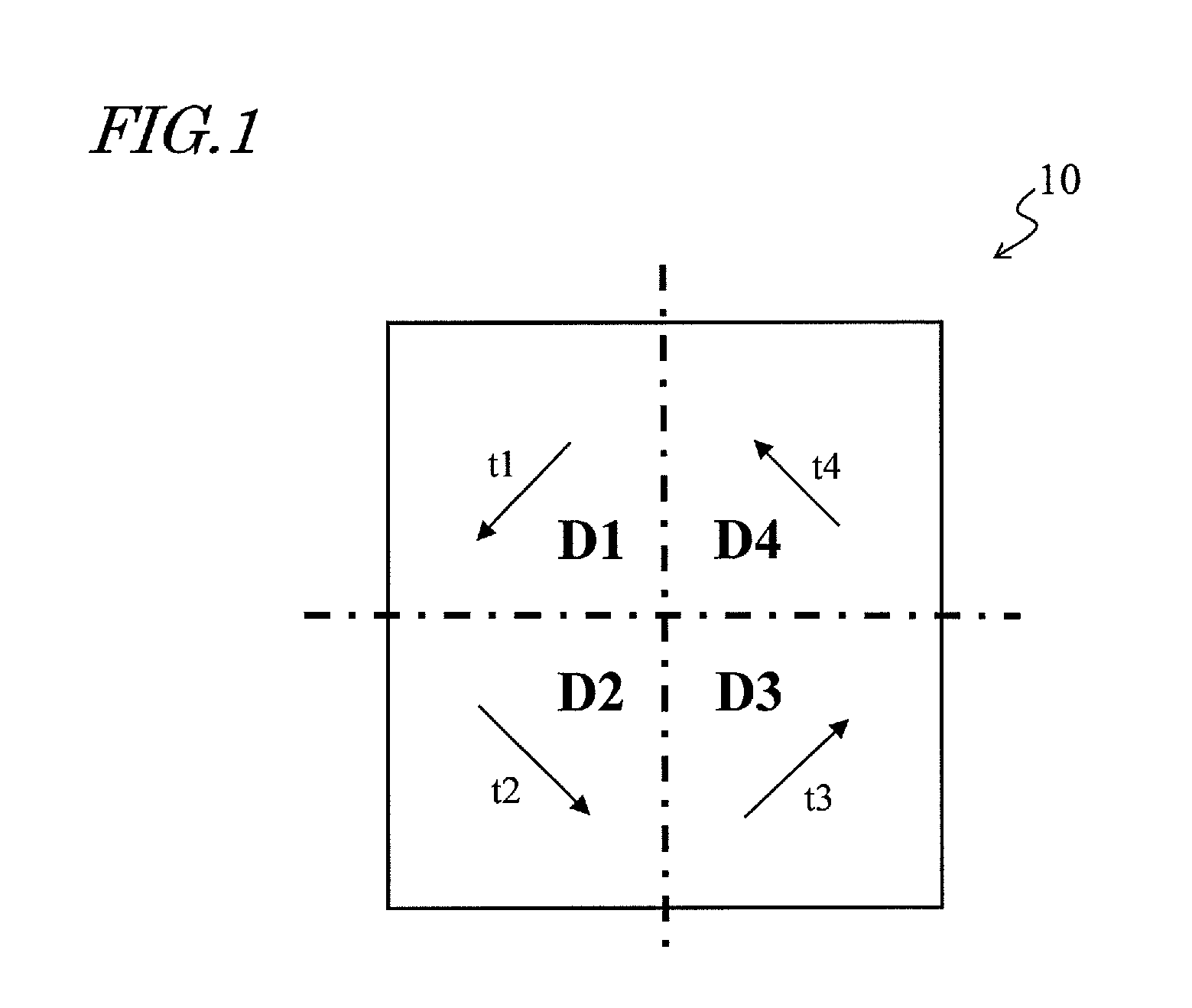
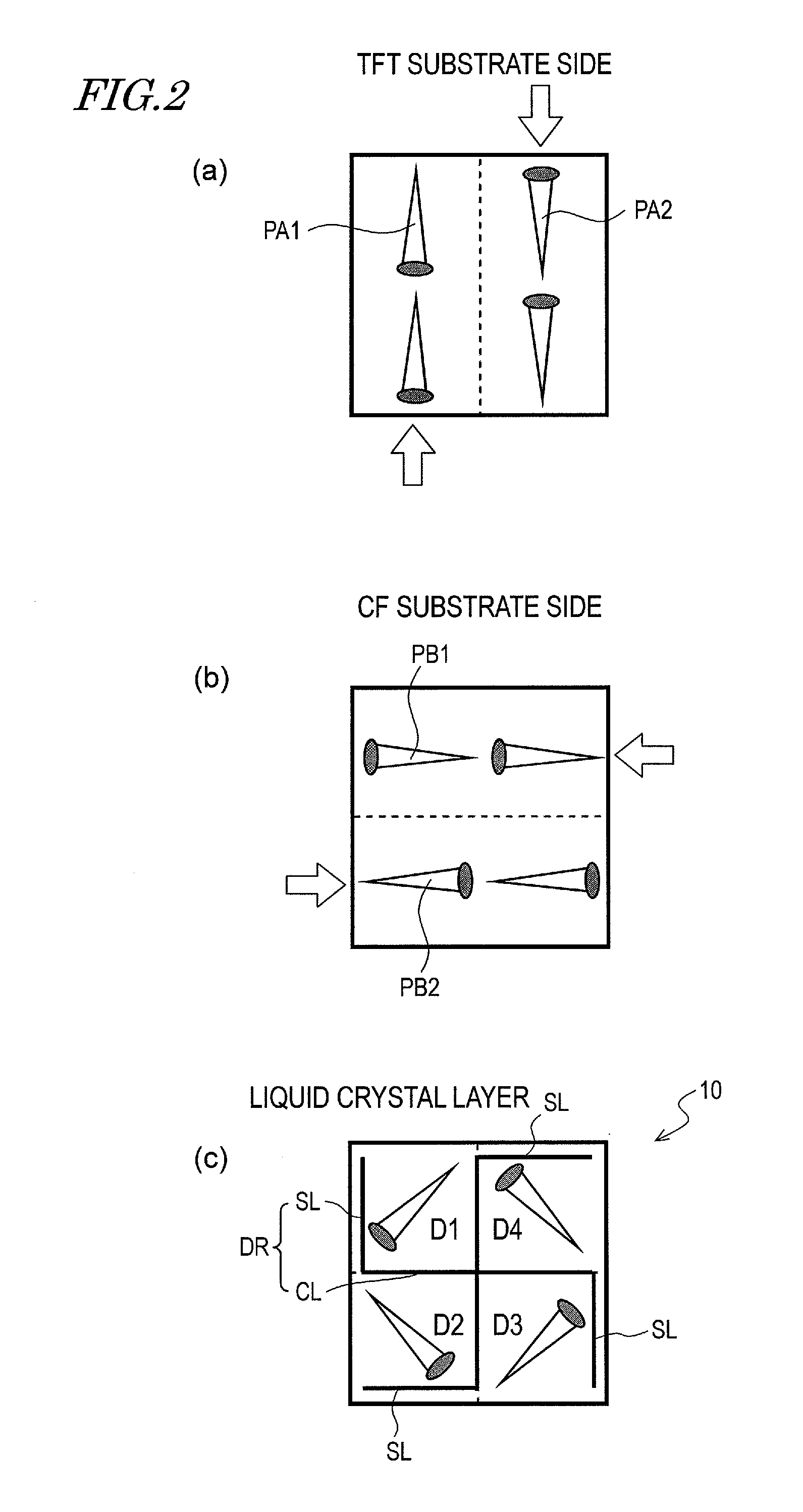
[0159]FIG. 1 shows a picture element 10 having a 4-domain alignment structure (4D structure). In FIG. 1, the picture element 10 is generally square in correspondence with a generally square picture element electrode for the sake of simplicity, but there is no limitation on the shape of the picture element. For example, the picture element 10 may be generally rectangular.

[0160]As shown in FIG. 1, the picture element 10 includes four liquid crystal domains D1, D2, D3 and D4. In FIG. 1, the liquid crystal domains D1, D2, D3 and D4 have an equal area size, and the example shown in FIG. 1 is the most preferable 4D structure from the viewpoint of viewing angle characteristics. The four liquid crystal...

embodiment 2

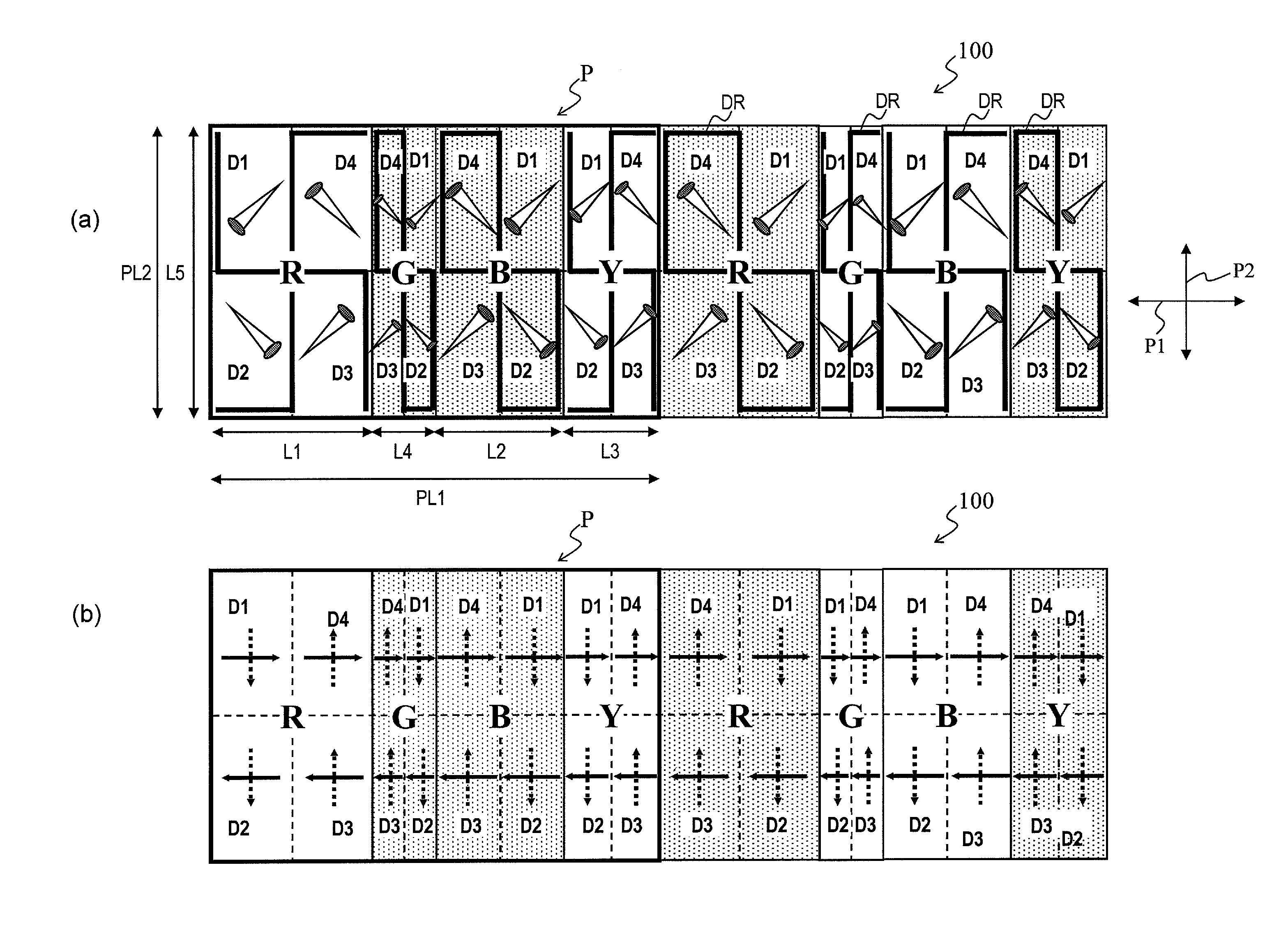
[0270]FIG. 44 shows a liquid crystal display device 200 in this embodiment. FIGS. 44(a) and (b) are each a plan view schematically showing four pixels P of the liquid crystal display device 200, which are continuous in the row direction.

[0271]As shown in FIGS. 44(a) and (b), all the four picture elements defining each pixel P have different lengths along the row direction. Specifically, a length L1 of the red picture element R along the row direction, a length L2 of the blue picture element B along the row direction, a length L3 of the yellow picture element Y along the row direction, and a length L4 of the green picture element G along the row direction are longer in this order (i.e., L1>L2>L3>L4). By contrast, all the picture elements have an equal length L5 along the column direction. In this manner, in the pixel P of the liquid crystal display device 200 in this embodiment, there is one length of picture elements in the column direction, whereas there are four lengths of picture...

embodiment 3

[0299]FIG. 51 shows a liquid crystal display device 300 in this embodiment. FIG. 51 is a plan view schematically showing six pixels P of the liquid crystal display device 300, which are continuous in the row direction.

[0300]As shown in FIG. 51, all the four picture elements defining each pixel P have different lengths along the row direction. Specifically, a length L1 of the red picture element R along the row direction, a length L2 of the blue picture element B along the row direction, a length L3 of the yellow picture element Y along the row direction, and a length L4 of the green picture element G along the row direction are longer in this order (i.e., L1>L2>L3>L4). By contrast, all the picture elements have an equal length L5 along the column direction. In this manner, in the pixel P of the liquid crystal display device 300 in this embodiment, there is one length of picture elements in the column direction, whereas there are four lengths of picture elements in the row direction....


PUM


Abstract

A liquid crystal display device (100) according to the present invention includes a vertical alignment type liquid crystal layer (3); and a pair of optical alignment films (12, 22). A plurality of picture elements (R, G, B, Y) each include four liquid crystal domains (D1 through D4) in which tilt directions of liquid crystal molecules when a voltage is applied are different. The four liquid crystal domains are located in a matrix of 2 rows×2 columns. The pair of optical alignment films have such an alignment regulation force that causes an identical alignment pattern to appear in repetition in the liquid crystal layer along a first direction which is parallel to one of a row direction and a column direction, with 2n pixels (n is an integer of 1 or greater) being a minimum unit. In the 2n pixels which form the repeat unit of alignment pattern, there are first picture elements and second picture elements in a mixed state, the first picture elements each including the four liquid crystal domains located in a first order, and the second picture elements each including the four liquid crystal domains located in a second order which is different from the first order. According to the present invention, when the 4D-RTN mode is adopted for a liquid crystal display device in which one pixel includes a picture element having a different size from that of another picture element, increase of the cost and the time which are required for optical alignment processing can be suppressed.

Description

TECHNICAL FIELD[0001]The present invention relates to a liquid crystal display device and a method for producing the same, and specifically a liquid crystal display device having a wide viewing angle characteristic and a method for producing the same.BACKGROUND ART[0002]Recently, liquid crystal display devices have been improved in terms of display characteristics, and are now used for TV receivers and the like more and more widely. The viewing angle characteristics of the liquid crystal display devices have been improved but are desired to be further improved. Especially, the viewing angle characteristics of liquid crystal display devices using a vertical alignment type liquid crystal layer (also referred to as “VA-mode liquid crystal display devices”) are strongly desired to be improved.[0003]VA-mode liquid crystal display devices currently used for large display devices of TVs and the like adopt a multi-domain structure in which a plurality of liquid crystal domains are formed in...

Claims


Application Information

Patent Timeline
IPC IPC(8): G02F1/1337G03F7/20G02F1/1335
CPCG02F1/133753G02F2201/52G02F2001/133742G02F1/133788G02F1/133742G02F1/1337G02F1/1335G02F1/1343
Inventor INOUE, IICHIROHMIYACHI, KOICHINAKAGAWA, HIDETOSHISHOHRAKU, AKIHIRO
Owner SHARP KK
Why Eureka
Try Eureka