Light emitting diode illumination display

a light-emitting diode and illumination display technology, applied in the field of display systems, can solve the problems of high total drive current, add to the overall system complexity, and reduce the overall system complexity, and achieve the effect of preventing substantial blurring of the imag

Inactive Publication Date: 2012-09-20
MCMASTER UNIV
View PDF6 Cites 35 Cited by
  • Summary
  • Abstract
  • Description
  • Claims
  • Application Information

AI Technical Summary

Benefits of technology

[0022]In another aspect, there is provided a display system comprising: one or more display modules as described above; and a rear-projection screen positioned to be illuminated by light transmitted by the optical modulating array layers of the one o...

Problems solved by technology

LED displays are bright and offer long life, however the resolution depends on the number of LEDs, and a high resolution screen requires a very large number of LEDs which is expensive and may result in reliability issues.
Also, each LED must be electronically addressed, which adds to the overall system complexity and very high total drive currents result.
In many applications where high resolution colour displays are used, this approach is not affordable.
Although highly successful, this technology has several limitations and disadvantages.
The overall display size is limited by the glass size of the LC modulator, and the brightness and efficiency are reduced by the use of colour filters.
In general, plasma and liquid crystal displays are not readily available in formats over about 2 meters in length due to their high weight, high cost and fragile nature.
They also suffer from lower power efficiencies (1-3 lumens/watt) which limits their suitability for high brightness, large size displays.
While this is beneficial for high-end display systems, the cost of providing the driving circuitry for each LED can be prohibitively expensive in many applications and market sectors.
A significant disadvantage of the aforementioned LED disp...

Method used


Image

  • Light emitting diode illumination display
  • Light emitting diode illumination display
  • Light emitting diode illumination display

Examples


examples

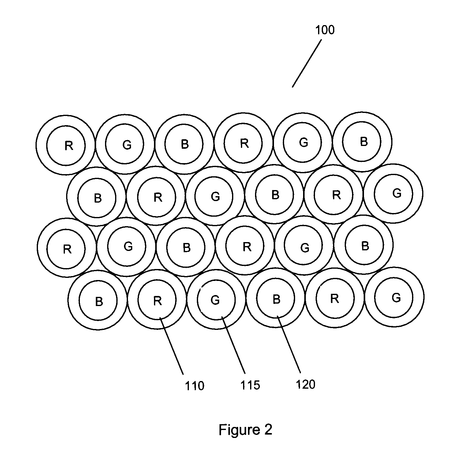
[0076]A display was constructed using an array of LED modules to illustrate an embodiment of the invention. FIG. 8(a) shows a schematic of a single LED module 300, without the LC modulator, in which twenty red 305, green 310 and blue 315 LEDs are contained. The LEDs are splayed both vertically and horizontally to allow LC modulators used in conjunction with the LED modules to be spaced apart. As shown in FIGS. 8(b) and 8(c), the maximum vertical splay is 12 degrees, while the maximum horizontal splay is 8 degrees. This splay allows the active areas of individual LC light modulators to be spaced approximately 12 mm apart in one dimension (the vertical dimension, as shown in the Figure) and 8 mm apart an another dimension (the horizontal dimension), which was a format compatible with the LCD selected for this specific design. FIG. 8(d) provides an isometric view of the LED array portion of the module, in which the open circles 320 represent the light cones produced by the red LEDs at ...


PUM


Abstract

A display illumination module for the illumination of a rear-projection screen is provided in which an array of light sources are positioned adjacent to an optical modulating array layer for modulating the transmission of light emitted by the light sources. The light sources emit light within a defined angular range, and the optical modulating array layer is positioned relative to the array of light sources so that light from adjacent light sources does not overlap with the optical modulating array layer. One or more display modules may be incorporated into a display system that further comprises a rear projection screen that is preferably spatially offset from the optical modulating array layer so that light from adjacent light sources of a common colour overlaps on the screen. A composite display with seamless edge blending may be obtained by tiling multiple display illumination modules behind a common rear-projection screen.

Description

CROSS-REFERENCE TO RELATED APPLICATION[0001]This application claims priority to U.S. Provisional Application No. 61 / 240,412 titled “LIGHT EMITTING DIODE ILLUMINATED DISPLAY” and filed on Sep. 8, 2009, the entire contents of which are incorporated herein by reference.FIELD OF THE INVENTION[0002]The present invention relates to display systems, and more particularly relates to modular liquid crystal display systems.BACKGROUND OF THE INVENTION[0003]Remarkable progress in light emitting diode (LED) technology has recently enabled high efficiency red, green and blue light sources with lifetimes of 100,000 hours. These are in current use for large indoor and outdoor video displays where each LED is directly viewed and electrically controlled. LED displays are bright and offer long life, however the resolution depends on the number of LEDs, and a high resolution screen requires a very large number of LEDs which is expensive and may result in reliability issues. Also, each LED must be elect...

Claims


Application Information

Patent Timeline
IPC IPC(8): G03B21/14G03B21/20G02F1/13357
CPCG02F1/133603G02F1/133606H04N9/3197H04N9/3164H04N9/3155G02F1/13336
Inventor KITAI, ADRIAN
Owner MCMASTER UNIV
Why Eureka
Try Eureka