LED package structure

a technology of light-emitting diodes and package structures, applied in the direction of basic electric elements, electrical equipment, semiconductor devices, etc., can solve the problems of increasing the manufacture cost of transparent encapsulants, the display cannot emit light by itself, etc., and achieves the effect of enhancing light extraction efficiency and increasing the diffusion angle of ligh

Active Publication Date: 2012-10-11
TCL CHINA STAR OPTOELECTRONICS TECH CO LTD
View PDF1 Cites 2 Cited by
  • Summary
  • Abstract
  • Description
  • Claims
  • Application Information

AI Technical Summary

Benefits of technology

[0010]A primary object of the present invention is to provide an LED package structure, which is formed with a plurality of protrusions in a recess of a housing or on an edge of the housing, so that a surface of a transparent encapsulant has an uneven profile to increase the diffusion angle of the light and enhance the light extraction efficiency.
[0011]Another object of the present invention is to provide an LED package structure, wherein different arrangements of the protrusions can further change and control the visual angle of light emitted by the LED package structure, so as to suitably satisfy different usage needs.

Problems solved by technology

However, the liquid crystal material of the liquid crystal display cannot emit light by itself, and must depend upon an external light source.
However, it will relatively increase the manufacture cost of the transparent encapsulant 95′.
Meanwhile, because the transparent encapsulant 95′ is protruded from the housing 91′, it is disadvantageous to execute the following SMT or other manufacturing processes of the LED package structure 90′.

Method used


Image

  • LED package structure
  • LED package structure
  • LED package structure

Examples


first embodiment

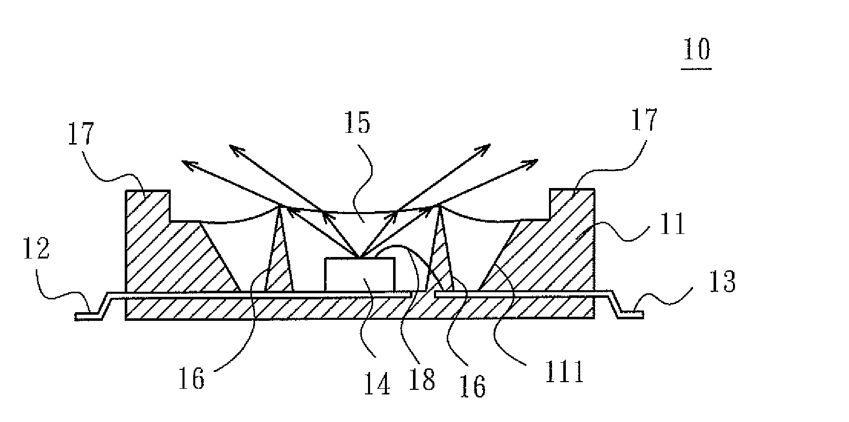
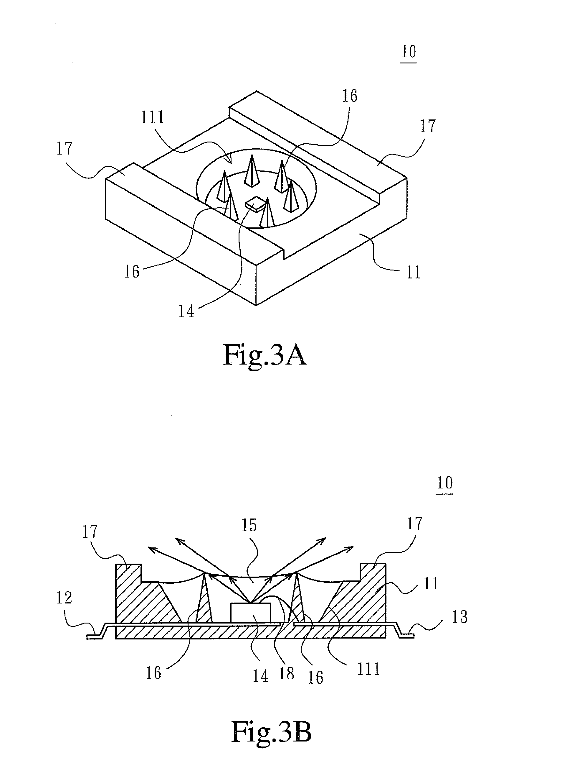
[0050]Furthermore, preferably, the housing 11 of the LED package structure 10 further comprises at least one protruded wall 17 which can be formed on the edge of the housing 11, wherein the height of the protruded wall 17 is greater than that of the protrusions 16. Thus, the protruded wall 17 of the LED package structure 10 in the present invention is advantageous to execute the following SMT or other manufacturing processes of the LED package structure 10.

[0051]For more details, due to the change of the surface shape of the transparent encapsulant 15, a pathway of a light beam emitted by the LED chip 14 through the transparent encapsulant 15 will be changed. As shown in FIG. 3B, the uneven surface of the transparent encapsulant 15 can decrease the ratio of total reflection of the light beam, so as to increase the diffusion angle thereof. Moreover, the light emitted to the protrusions 16 will be reflected from the reflective layer on the surface of the protrusions 16, and then emitt...

fourth embodiment

[0057]Furthermore, preferably, the height of the protrusions 46 of the LED package structure 40 is greater than that of the transparent encapsulant 45. Thus, the protrusions 46 of the LED package structure 40 in the present invention is advantageous to execute the following SMT or other manufacturing processes of the LED package structure 40.

[0058]For more details, in the embodiment, the LED package structure 40 can provide the same technological effect of the LED package structure 10 in the first embodiment of the present invention. In the embodiment, due to the protrusions 46, the surface shape of the transparent encapsulant 45 of the LED package structure 40 are changed, and thus a pathway of a light beam emitted through the transparent encapsulant 45 will be changed. As shown in FIG. 6B, the uneven surface of the transparent encapsulant 45 can generate an effect of a convex lens. Thus, most of the light beam is emitted outward through the transparent encapsulant 45, so as to inc...


PUM


Abstract

The present invention discloses an LED package structure which has a housing, an LED chip and a transparent encapsulant. The housing has a recess and a plurality of protrusions. The LED chip is mounted in the recess of the housing, and covered in the recess by the transparent encapsulant. The protrusions are formed in the recess or on the edge of the housing. The protrusions of the present invention can form the uneven shape of the surface of the transparent encapsulant, so as to increase the diffusion angle of the light and enhance the light extraction efficiency.

Description

FIELD OF THE INVENTION[0001]The present invention relates to a light emitting diode (LED) package structure, and more particularly to an LED package structure having a transparent encapsulant with an uneven surface.BACKGROUND OF THE INVENTION[0002]A liquid crystal display (LCD) is a type of flat panel display (FPD), which shows images by the property of liquid crystal material. Comparing with other display devices, the liquid crystal display has advantages in lightweight, compactness, low driving voltage and low power consumption, and thus has already become the mainstream product in the whole consumer market. However, the liquid crystal material of the liquid crystal display cannot emit light by itself, and must depend upon an external light source. Thus, the liquid crystal display further has a backlight module to provide the needed light source.[0003]Generally, the backlight module can be divided into two types, i.e. the side-light type backlight module and the direct-light type ...

Claims


Application Information

Patent Timeline
Patent Type & Authority Applications(United States)
IPC IPC(8): H01L33/60
CPCH01L33/60H01L33/54
Inventor CHANG, KUANGYAOZHENG, WEIWEI
Owner TCL CHINA STAR OPTOELECTRONICS TECH CO LTD
Why Eureka
Try Eureka