

Photoelectric conversion device and method of preparing the same
- Summary
- Abstract
- Description
- Claims
- Application Information
AI Technical Summary
Benefits of technology
Problems solved by technology
Method used
Image

Examples
first embodiment
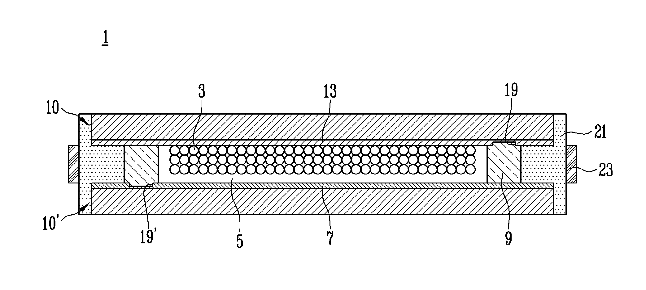
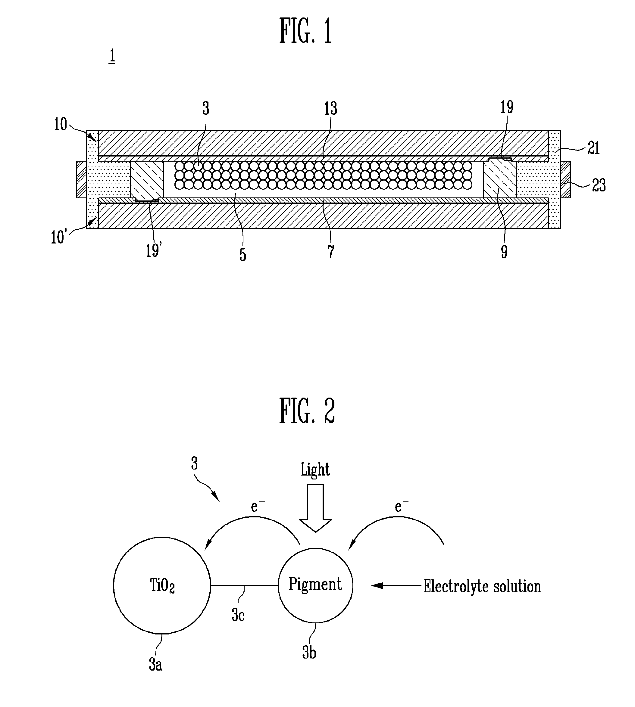
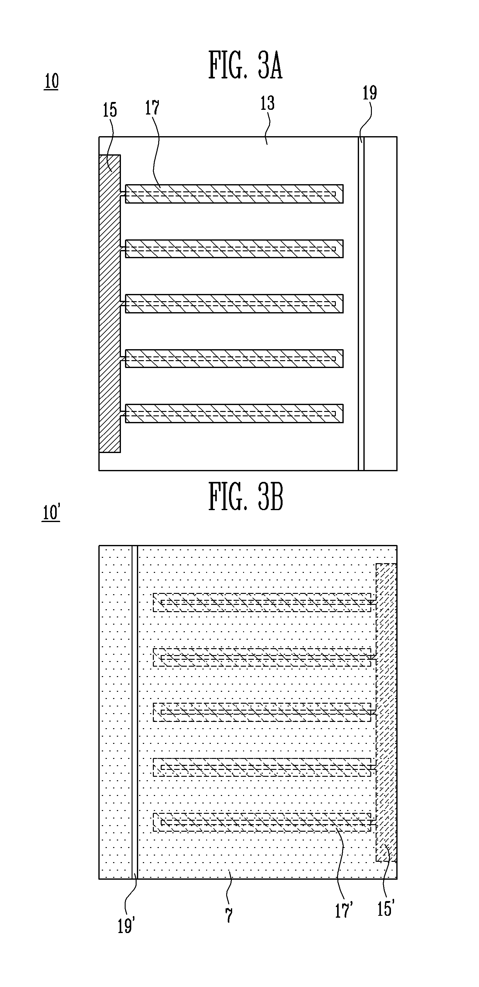
[0051]Referring to FIGS. 4A and 4B, a first non-slip portion 19a according to the present disclosure may be a trench formed in the transparent electrode layer 13 and a second non-slip portion 19a′ may be a trench formed in the counter electrode layer 7.
[0052]Therefore, the transparent electrode layer 13 and the counter electrode layer 7 are exposed through bottoms of the trenches. Here, the trench may be formed by projecting laser but methods of forming the trench are not limited thereto.
[0053]Meanwhile, a conductive material layer 21 may be further formed at the outer side of the sealing member 9 and between the first substrate 10 and the second substrate 10′ and form of a desired conductive material layer 21 is completed by pressing in the arrow direction. A connecting terminal 23 connected to the conductive material layer 21 may be further formed. Referring to FIG. 8, the connecting terminal 23 is electrically connected to the outside of the photoelectric conversion device 1 to r...
second embodiment
[0055]Referring to FIGS. 5A and 5B, a first non-slip portion according to the present disclosure may be a trench formed on the first substrate by passing through the transparent electrode layer 13 and a second non-slip portion 19b′ may be a trench formed on the second substrate 10′ by passing through the counter electrode layer 7.
[0056]Therefore, the first substrate 10 and the second substrate 10′ are exposed through bottoms of the trenches. Here, the trench may be formed by projecting laser but method of forming the trench is not limited thereto.
[0057]A conductive material layer 21 may be further formed at the outer side of the sealing member 9 and in a space between the first substrate 10 and the second substrate 10′ and form of a desired conductive material layer 21 is completed by pressing in the arrow direction. Next, a connecting terminal 23 connected to the conductive material layer 21 may be further formed. Referring to FIG. 8, the connecting terminal 23 may be electrically ...
third embodiment
[0060]Referring to FIGS. 6a and 6B, a first non-slip portion 19c according to the present disclosure may be a trench formed in the transparent electrode layer 13 and a second non-slip portion 19c′ may be a trench formed in the counter-electrode layer 7. Therefore, the transparent electrode layer 13 and the counter electrode layer 7 are exposed through bottoms of the trenches. Here, the trench may be formed by projecting laser but methods of forming the trench are not limited thereto.
[0061]Meanwhile, surfaces of the first substrate 10 and the second substrate 10′ facing the sealing member 9 are cut away. Therefore, more quantity of a conductive material layer 31 may be further formed at the outer side of the sealing member 9 and in a wider area between the first substrate 10 and the second substrate 10′ and form of a desired conductive material layer 31 is completed by pressing in the arrow direction. A connecting terminal 33 electrically connected to the conductive material layer 31...
PUM
 Abstract
Description
Claims
Application Information