Optical proximity correction method based on hybrid simulation model

Active Publication Date: 2014-10-14
SHANGHAI HUALI MICROELECTRONICS CORP
View PDF4 Cites 3 Cited by
  • Summary
  • Abstract
  • Description
  • Claims
  • Application Information

AI Technical Summary

Benefits of technology

[0015]As described herein, the OPC method of the present invention provides a number of benefits over the prior art OPC method. For example, by grouping the original patterns into the larger-sized ones and smaller-sized ones and establishing in

Problems solved by technology

However, due to continuing shrinkage of critical dimensions of the semiconductor devices as well as resolution limits of exposure tools, a phenomenon referred as optical proximity effect (OPE) is prone to occur when to expose and transfer mask patterns arranged with a high density.
This OPE effect can lead to defects when transferring the mask patterns onto the chip, common examples of which include right-angled corner rounding, line end shortening and line-width variations (including both increases and decreases).
On the othe

Method used


Image

  • Optical proximity correction method based on hybrid simulation model
  • Optical proximity correction method based on hybrid simulation model
  • Optical proximity correction method based on hybrid simulation model

Examples


Embodiment Construction

[0020]The present invention will be further described with reference to the following detailed description of exemplary embodiments, taken in conjunction with the accompanying drawings. Features and advantages of the invention will be apparent from the following detailed description, and from the claims. Note that all the drawings are presented in a very simple form and not drawn precisely to scale. They are provided solely to facilitate the description of the exemplary embodiments of the invention in a convenient and clear way.

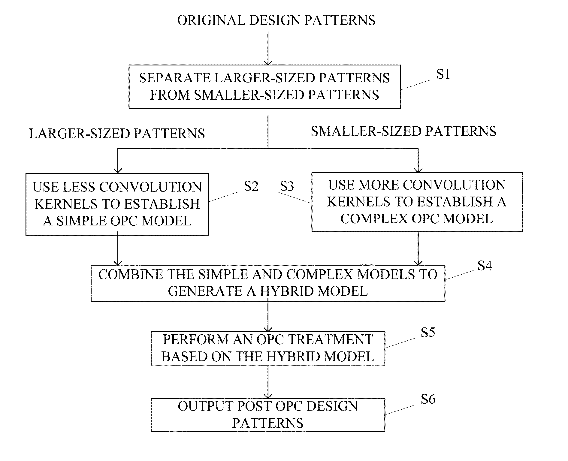
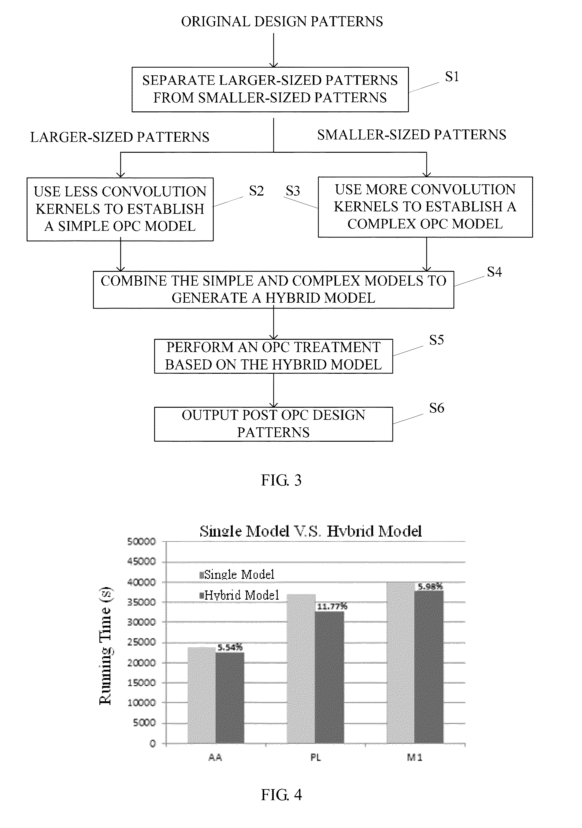
[0021]FIG. 3 illustrates process steps (S1 to S6) of an optical proximity correction (OPC) method in accordance with one embodiment of the present invention.

[0022]In step S1, original design patterns are grouped into a first group and a second group by their sizes.

[0023]The original design patterns are of a layout designed for a given semiconductor device fabrication process and provide a basis for wafer fabrication.

[0024]The original design patterns are grou...


PUM


Abstract

An optical proximity correction (OPC) method is disclosed, in which original design patterns are first grouped into a first group and a second group, wherein each pattern of the first group has a size greater than a size of any pattern of the second group. Next, a simple OPC model and a complex OPC model are individually established for the two groups using different numbers of convolution kernels. After that, the simple OPC model and the complex OPC model are combined together to generate a hybrid OPC model which is thereafter used to perform an OPC treatment on the original design patterns. This method is capable of shortening the OPC processing time and increasing the flexibility in utilizing OPC software and hardware resources.

Description

CROSS-REFERENCES TO RELATED APPLICATIONS[0001]This application claims the priority of Chinese patent application, number 2013 10229404.3, filed on Jun. 8, 2013, the entire contents of which are incorporated herein by reference.TECHNICAL FIELD[0002]The present invention relates generally to the field of semiconductor device fabrication, and more particularly to an optical proximity correction (OPC) method.BACKGROUND[0003]In general terms, a process for fabricating a semiconductor device involves transferring an integrated circuit (IC) layout to a semiconductor chip, which typically includes: first forming the IC layout on a mask to form a mask pattern thereon; and then transferring the mask pattern onto the semiconductor chip.[0004]However, due to continuing shrinkage of critical dimensions of the semiconductor devices as well as resolution limits of exposure tools, a phenomenon referred as optical proximity effect (OPE) is prone to occur when to expose and transfer mask patterns arr...

Claims


Application Information

Patent Timeline
IPC IPC(8): G06F17/50G03F1/36
CPCG03F1/36G06F17/5068
Inventor CHEN, HANWEI, FANGCHANG, HSUSHENGCHU, ZHIHAO
Owner SHANGHAI HUALI MICROELECTRONICS CORP
Why Eureka
Try Eureka