Resonance nanoelectromechanical systems

a nano-electromechanical and nano-electromechanical technology, applied in the field of nano-electromechanical systems, can solve the problems of nems devices not being as reliable as cmos counterparts, implementing nems technology, etc., and achieve the effect of faster refresh rates

Inactive Publication Date: 2012-10-25
GLOBALFOUNDRIES US INC
View PDF4 Cites 9 Cited by
  • Summary
  • Abstract
  • Description
  • Claims
  • Application Information

AI Technical Summary

Benefits of technology

[0005]An example embodiment of the present invention is a NEMS switch involving a nanometer-scale cantilever beam anchored to a fixed end, while the beam's free end is proximate a gate electrode and a drain electrode. A drive circuit sends an AC modulated drive signal through the gate electrode, creating a gate voltage, which results in a pull-down force on the cantilever beam, thereby bringing the beam into contact with the drain electrode. By operating the AC modulated drive signal at or near the beam's resonance frequency, the beam may achieve a steady-state motion, whereby the beam oscillates at or near its resonance frequency. This beam's amplitude of motion may be larger than where the beam moved at other frequencies. A larger amplitude of motion may provide that less gate voltage may be necessary to operate the NEMS switch.
[0007]Another example embodiment of the present invention is a NEMS switch involving a nanometer-scale cantilever beam anchored to a fixed end, where the beam's free end is proximate a gate electrode and a plurality of drain regions. Where a drive circuit applies a voltage to the gate electrode, the cantilever beam may contact different drain surface regions while oscillating. Allowing contact with a plurality of drain regions may enable faster refresh rates by utilizing the beam's away motion to contact a drain region as well as the beam's returning motion to contact a drain region.

Problems solved by technology

Despite some possible advantages, there exist several problems for implementing NEMS technology.
Second, NEMS devices may not be as reliable as their CMOS counterparts.

Method used


Image

  • Resonance nanoelectromechanical systems
  • Resonance nanoelectromechanical systems
  • Resonance nanoelectromechanical systems

Examples


Embodiment Construction

[0018]The present invention is described with reference to various embodiments of the invention. Throughout the description of the invention reference is made to FIGS. 1-6.

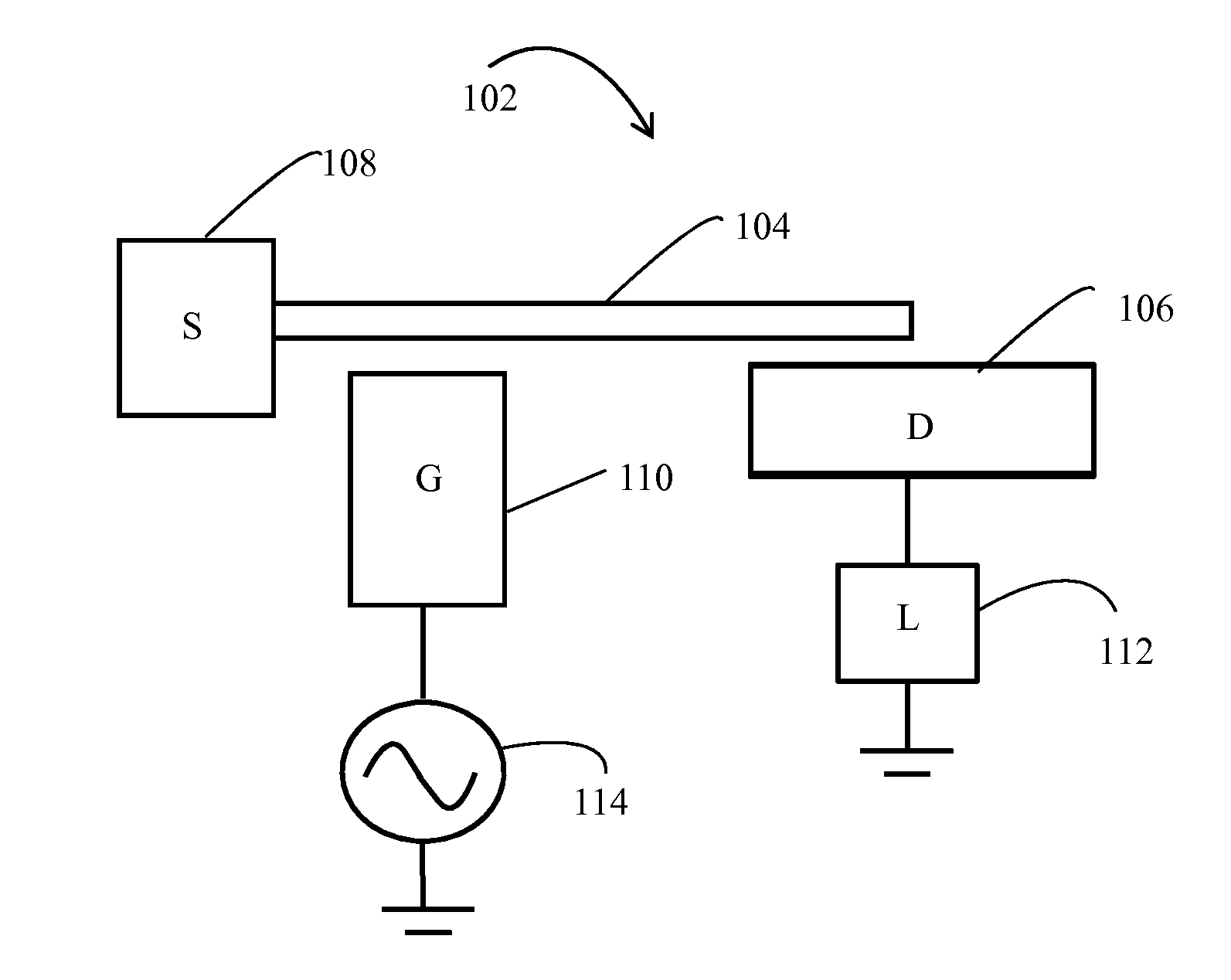
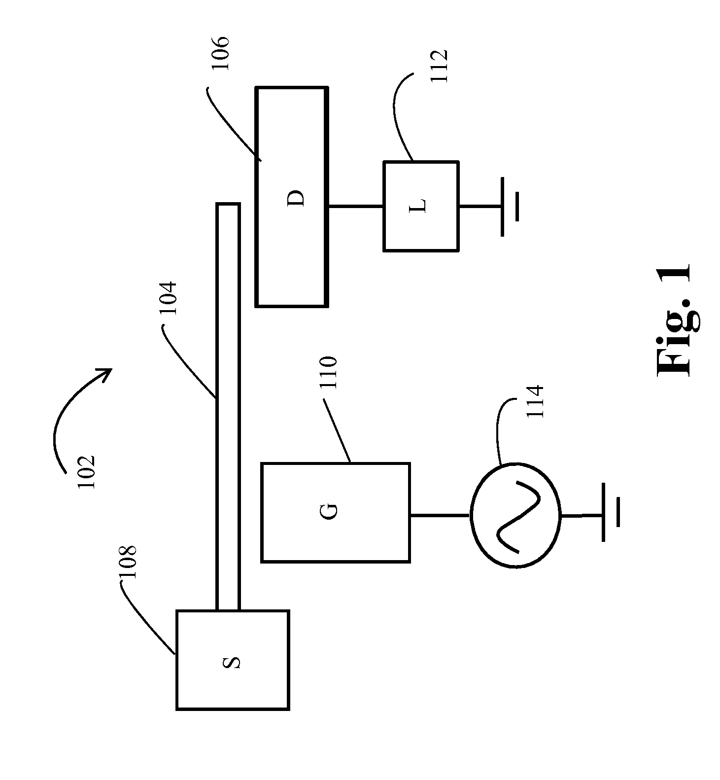
[0019]FIG. 1 is a schematic drawing of a nanoelectromechanical system (NEMS) 102 showing one embodiment of the present invention. The system 102 includes a gate electrode 110, which is proximate a nanometer-scale cantilever beam 104, where the cantilever beam 104 has a resonance frequency, where the resonance frequency and resonant frequency are interchangeable terms. A drive circuit 114 is coupled to the gate electrode 110, and the drive circuit 114 is configured to apply a drive signal to the gate electrode 110.

[0020]Furthermore, this inventive embodiment in FIG. 1 may include a cantilever beam 104 with a fixed end and a free end. At the fixed end, the cantilever beam 104 may couple to a source electrode 108. Proximate the free end, the NEMS 102 may comprise a drain electrode 106, such that the cantilever beam 1...


PUM


Abstract

Systems and methods for operating a nanometer-scale cantilever beam with a gate electrode. An example system includes a drive circuit coupled to the gate electrode where a drive signal from the circuit may cause the beam to oscillate at or near the beam's resonance frequency. The drive signal includes an AC component, and may include a DC component as well. An alternative example system includes a nanometer-scale cantilever beam, where the beam oscillates to contact a plurality of drain regions.

Description

BACKGROUND[0001]This invention relates to nanoelectromechanical systems (NEMS). More particularly, the present invention relates to a method for operating a NEMS device at or near its resonance frequency, a system that operates a NEMS device at or near its resonance frequency, and a system for operating a nanometer-scale cantilever with multiple drain regions.[0002]Many memory cell devices use transistors to read and write data, but NEMS devices offer an alternative approach to performing this task. For example, because a NEMS switch is a mechanical switch, a NEMS-based memory cell can be in an OFF state without an existing off current. This is a valuable advantage over competing complimentary metal-oxide semiconductor (CMOS) technology. Because no off current, a NEMS switch may allow for a lower standby leakage current. NEMS switches may have better sub-threshold behavior than transistors, which are typically limited to 60 mV / dec. Using a NEMS switch may also provide for a sharper ...

Claims


Application Information

Patent Timeline
Patent Type & Authority Applications(United States)
IPC IPC(8): G11C11/50H03B5/30
CPCH03H9/2457G11C23/00G11C11/404H03H2009/02314
Inventor CHANG, LELANDGUILLORN, MICHAEL A.GUO, DECHAOLIU, FEIWONG, KEITH KWONG HON
Owner GLOBALFOUNDRIES US INC
Why Eureka
Try Eureka