

Acoustic wave device
- Summary
- Abstract
- Description
- Claims
- Application Information
AI Technical Summary
Benefits of technology
Problems solved by technology
Method used
Image

Examples
exemplary embodiment 1
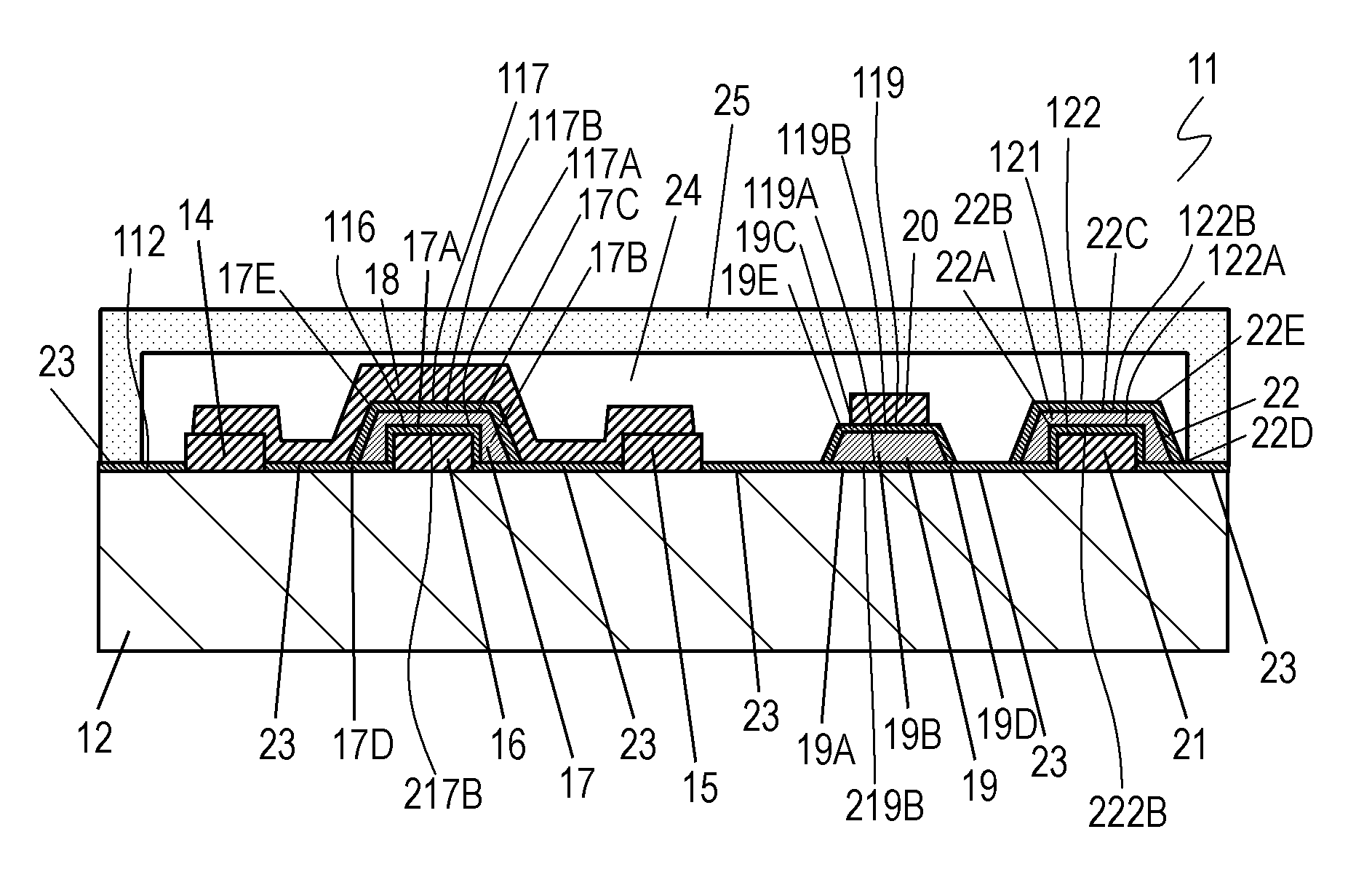
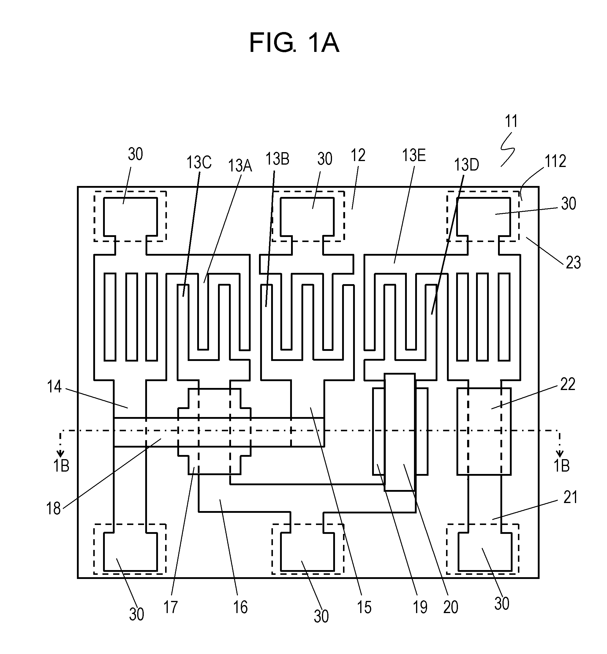
[0021]FIG. 1A is a top view of a piezoelectric substrate 12 of an acoustic wave device 11 according to Exemplary Embodiment 1 of the present invention. FIG. 1B is a cross sectional view of the acoustic wave device 11 along line 1B-1B shown in FIG. 1A.
[0022]The acoustic wave device 11 includes the piezoelectric substrate 12 and comb-shaped electrodes 13A to 13E disposed on an upper surface 112 of the piezoelectric substrate 12. The piezoelectric substrate 12 is made of a single crystal piezoelectric substance, such as lithium tantalate or lithium niobate. The comb-shaped electrodes 13A to 13E are arranged to excite an acoustic wave on the piezoelectric substrate 12 to allow the acoustic wave device 11 to constitute a filter circuit. The acoustic wave device 11 further includes wirings 14, 15, 16, 20, and 21 which are connected to the comb-shaped electrodes 13A, 13B, 13C, 13D, and 13E, respectively. The wirings 14, 15, 16, and 21 are disposed on the upper surface 112 of the piezoelect...
exemplary embodiment 2
[0045]FIG. 2A is an upper view of the piezoelectric substrate 12 of an acoustic wave device 61 according to Exemplary Embodiment 2 of the present invention. FIG. 2B is a cross sectional view of the acoustic wave device 61 along lines 2B-2B shown in FIG. 2A. FIG. 2C is a cross sectional view of the acoustic wave device 61 along line 2C-2C shown in FIG. 2A. In FIGS. 2A to 2C, components identical to those of the acoustic wave device 11 according to Embodiment 1 shown in FIGS. 1A to 1D are denoted by the same reference numerals.
[0046]The acoustic wave device 61 according to Embodiment 2 is different from the acoustic wave device 11 according to Embodiment 1 in that a wiring and an organic insulator are covered with a single inorganic insulator and face an oscillation space 24 across the inorganic insulator.
[0047]In the acoustic wave device 61, wirings 16 and 18 on the upper surface 112 of the piezoelectric substrate 12 cross one over the other across an organic insulator 26 between wir...
PUM
 Abstract
Description
Claims
Application Information