Supercharge Your Innovation With Domain-Expert AI Agents!

Semiconductor light emitting structure

a technology of light-emitting structure and semiconductor, applied in the field of light-emitting elements, can solve the problems of unsatisfactory light extraction efficiency and emission, and achieve the effect of increasing light reflection and scattering, and increasing light extraction efficiency

Active Publication Date: 2012-11-29
LEXTAR ELECTRONICS CORP
View PDF2 Cites 4 Cited by
  • Summary
  • Abstract
  • Description
  • Claims
  • Application Information

AI Technical Summary

Benefits of technology

The invention is a semiconductor structure that increases the reflection and scattering of light to improve its extraction efficiency. This is achieved by creating a patterned structure on the substrate surface, which makes the surface rough and results in an asymmetrical geometric shape. The first semiconductor layer is then placed on the rough surface, followed by the active layer and finally the second semiconductor layer. The patterned structure can have various shapes, such as scalene triangle, scalene trapezoid, scalene, non-parallel polygon, or arc with variant curvature. Overall, this structure improves the performance of semiconductor light emitting devices.

Problems solved by technology

As most of the light is confined in the substrate, the light cannot be emitted out, and the light extraction efficiency is not satisfactory.

Method used


Image

  • Semiconductor light emitting structure
  • Semiconductor light emitting structure
  • Semiconductor light emitting structure

Examples


first embodiment

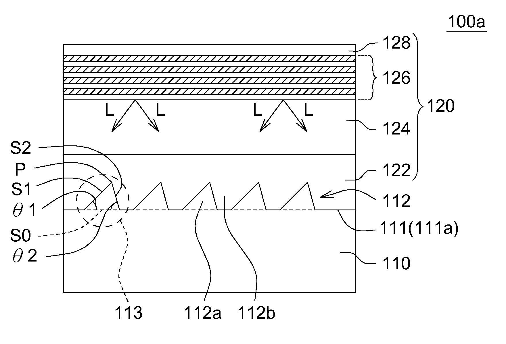
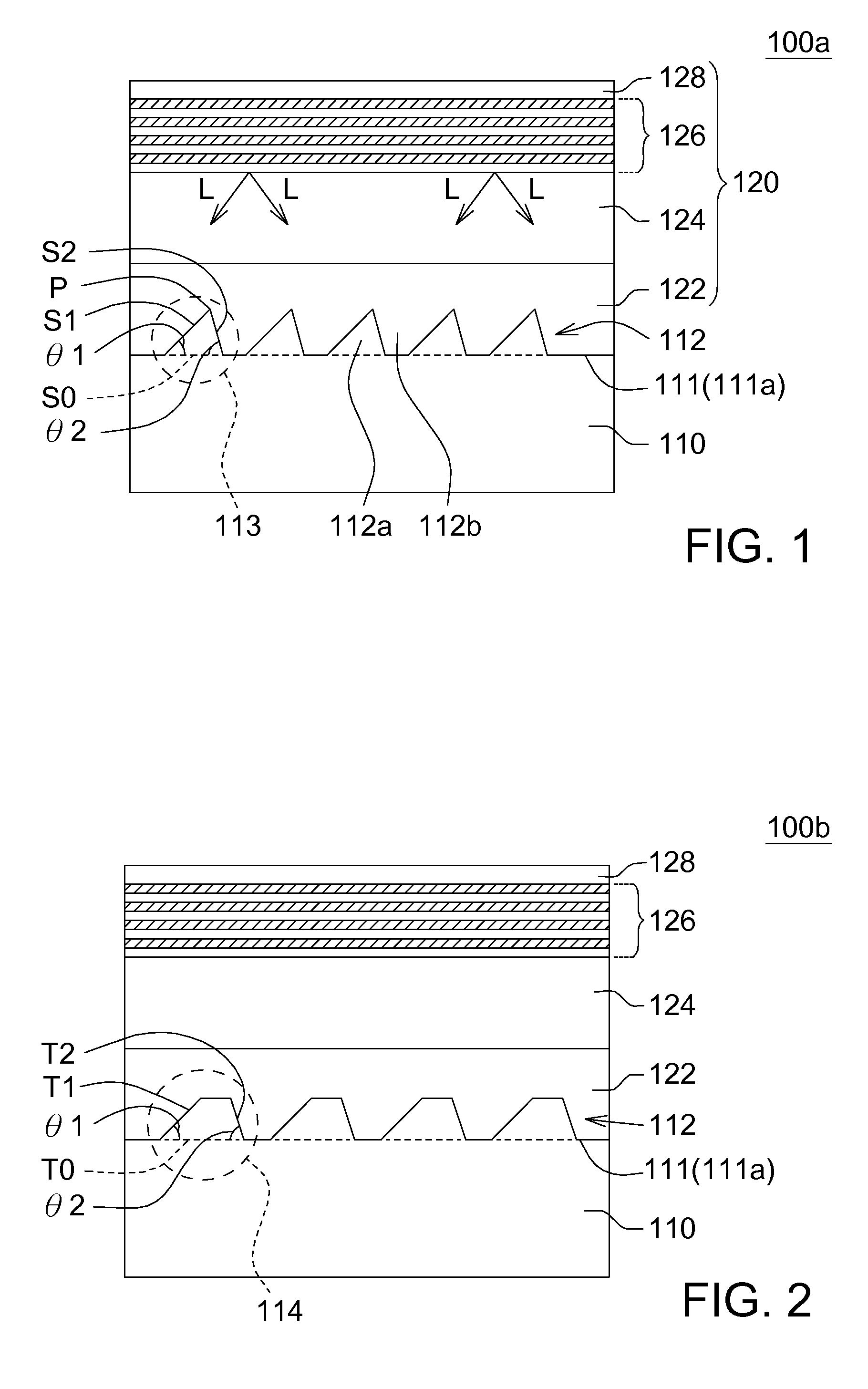
[0020]Referring to FIG. 1, a schematic diagram of a semiconductor light emitting structure according to an embodiment of the invention is shown. The semiconductor light emitting structure 100a includes a substrate 110, a patterned structure 112, a first semiconductor layer 124, an active layer 126 and a second semiconductor layer 128. The patterned structure 112 is protruded from or indented into a surface 111 of the substrate 110, so that the surface 111 of the substrate 110 becomes a roughed surface 111a. The patterned structure 112 has an asymmetrical geometric shape (circled with a dotted line 113). The first semiconductor layer 124 is disposed on the roughed surface 111a. The active layer 126 is disposed on the first semiconductor layer 124. The second semiconductor layer 128 is disposed on the active layer 126.

[0021]In the present embodiment of the invention, the patterned structure 112 is formed on the surface 111 of the substrate 110 through anisotropic etching process or re...

second embodiment

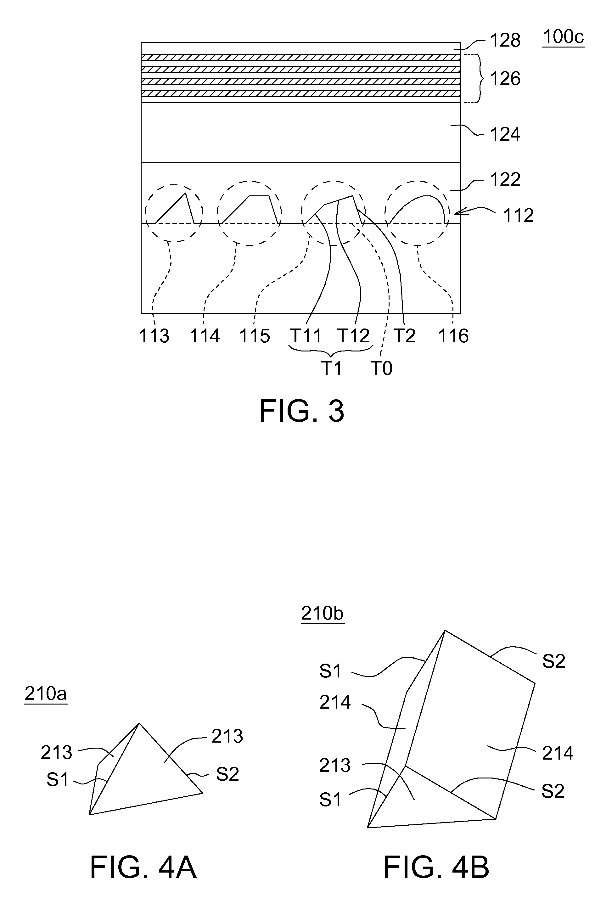
[0028]FIG. 4A˜4D respectively show 3D diagrams of a patterned structure 112 according to an embodiment of the invention. For the purpose of simplification, only the structure with one single patterned state is illustrated. However, the scope of protection of the invention is not limited thereto, and the structure with several patterned states arranged at random or with regularity is also within the scope of protection of the invention.

[0029]Referring to FIGS. 4A and 4B, asymmetrical geometric shapes such as triangular pyramid 210a or triangular prism 210b are shown. As indicated in FIG. 4A, the triangular pyramid 210a is composed of three scalene triangles 213 intersecting with each other at the vertex, wherein each scalene triangle 213, such as the scalene triangle 113 of the first embodiment (referring to FIG. 1), has two unequal lateral sides S1 and S2. As indicated in FIG. 4B, the triangular prism 210b is composed of two scalene triangles 213 and two scalene quadrilaterals 214, ...

third embodiment

[0031]Referring to FIG. 5, a schematic diagram of a patterned substrate according to an embodiment of the invention is shown. The patterned substrate 310 can be realized by a substrate made from sapphire substrate, silicon carbide substrate or silicon substrate. Despite only the patterned substrate 310 is illustrated in the present embodiment, the scope of protection of the invention is not limited thereto. Like the first embodiment, in the present embodiment of the invention, the first semiconductor layer 124 can be disposed on the surface 311 of the patterned substrate 310. Then, the active layer 126 is disposed on the first semiconductor layer 124, and the second semiconductor is disposed on the active layer 126 to form a semiconductor light emitting structure.

[0032]The present embodiment is different from the above embodiments in that the patterned structure 312 is distributed on the surface 311 of the patterned substrate in the shape of strips rather than islands. The patterned...


PUM


Abstract

A semiconductor light emitting structure including a substrate, a patterned structure, a first semiconductor layer, an active layer and a second semiconductor layer is provided. The patterned structure is protruded from or indented into a surface of the substrate, so that the surface of the substrate becomes a roughed surface. The patterned structure has an asymmetrical geometric shape. The first semiconductor layer is disposed on the roughed surface. The active layer is disposed on the first semiconductor layer. The second semiconductor is disposed on the active layer.

Description

[0001]This application claims the benefit of Taiwan application Serial No. 100117993, filed May 23, 2011, the subject matter of which is incorporated herein by reference.BACKGROUND OF THE INVENTION[0002]1. Field of the Invention[0003]The invention relates in general to a light emitting element, and more particularly to a semiconductor light emitting structure with a patterned structure.[0004]2. Description of the Related Art[0005]Light emitting diode (LED) emits the light through photoelectron conversion. The main constituting material of the light emitting diode is semiconductor, wherein the semiconductor with a higher ratio of holes carrying positive charges is referred as a P-type semiconductor, and the semiconductor with a higher ratio of electrons carrying negative charges is referred as an N-type semiconductor. A PN joint is formed at the junction between the P-type semiconductor and the N-type semiconductor. When voltages are applied to the positive electrode and the negative...

Claims


Application Information

Patent Timeline
Patent Type & Authority Applications(United States)
IPC IPC(8): H01L33/02H01L33/22
CPCH01L2933/0091H01L33/20
Inventor YU, CHANG-CHINLIN, MONG-EA
Owner LEXTAR ELECTRONICS CORP
Features
  • R&D
  • Intellectual Property
  • Life Sciences
  • Materials
  • Tech Scout
  • Unparalleled Data Quality
  • Higher Quality Content
  • 60% Fewer Hallucinations
Learn More