Mounting board and structure of the same

a technology of mounting plate and mounting plate, which is applied in the direction of semiconductor devices, solid-state devices, printed circuit details, etc., can solve the problems of low strength of the overhang portion of the wiring plate b>24/b>, affecting the appearance of the solder, etc., so as to facilitate visual inspection and easy mounting. , the effect of easy adaptation

Active Publication Date: 2012-12-13
CITIZEN WATCH CO LTD +2
View PDF6 Cites 12 Cited by
  • Summary
  • Abstract
  • Description
  • Claims
  • Application Information

AI Technical Summary

Benefits of technology

[0016]The mounting board of the present invention for mounting thereon an electronic component has an upper surface, a lower surface, a pass-through hole penetrating the upper surface and the lower surface, a peripheral side surface that defines the pass-through hole, and at least one pair of patterned electrodes extending along the pass-through hole from the upper surface to the lower surface across the peripheral side surface. On the other hand, the upper surface of the substrate of the electronic component is mounted on the lower surface of the mounting board, and at least part of at least one pair of patterned electrodes provided on the upper surface of the substrate of the electronic component is disposed to be located inside the pass-through hole past the peripheral side surface that defines the pass-through hole of the mounting board. The electronic component is mounted on the mounting board inside the peripheral side surface that defines the pass-through hole by soldering an electrically conductive portion to the connection of a patterned electrode. Accordingly, when viewed from above the upper surface of the mounting board, a solder fillet or a connection portion is seen within the pass-through hole, allowing the condition of the solder to be visually checked with ease.
[0017]Furthermore, the plurality of patterned electrodes provided along the pass-through hole of the mounting board are split into a plurality of independent patterned electrodes by a plurality of penetrating grooves which are cut into the mounting board so as to penetrate through the upper and lower surfaces from the peripheral side surface that defines the pass-through hole. Accordingly, the mounting board can be easily adapted only by modifying the number and position of penetrating grooves to various electronic component substrates having different numbers and positions of patterned electrodes.
[0018]Furthermore, the mounting board of the present invention can be used to easily mount thereon even an electronic component such as a light-emitting diode with a metal base in which a through hole electrode is difficult to form. Furthermore, the mounting board can be provided on the upper surface thereof with a patterned conductor for circuit wiring in order to provide a sufficient dielectric strength distance between the patterned conductor and the electronic component, thereby providing enhanced reliability.
[0019]Furthermore, for a light-emitting diode employed as the electronic component, most of the patterned electrodes or the like on the light emission side of the light-emitting diode are to be hidden below the mounting board. It is thus possible to visually simplify the outer appearance of the light emission side of the light-emitting diode.

Problems solved by technology

However, a light-emitting diode with a substrate having a metal base such as of aluminum and a wiring plate superimposed one on the other would be more expensive than one with an insulating substrate because it is difficult to provide the patterned electrodes extending around the side surfaces and the through hole electrodes.
Furthermore, the overhang portion of the wiring plate 24 had a low strength and thus tended to be damaged when subjected to, for example, the weight of the base 22 or the heat sink 30.

Method used


Image

  • Mounting board and structure of the same
  • Mounting board and structure of the same
  • Mounting board and structure of the same

Examples


first embodiment

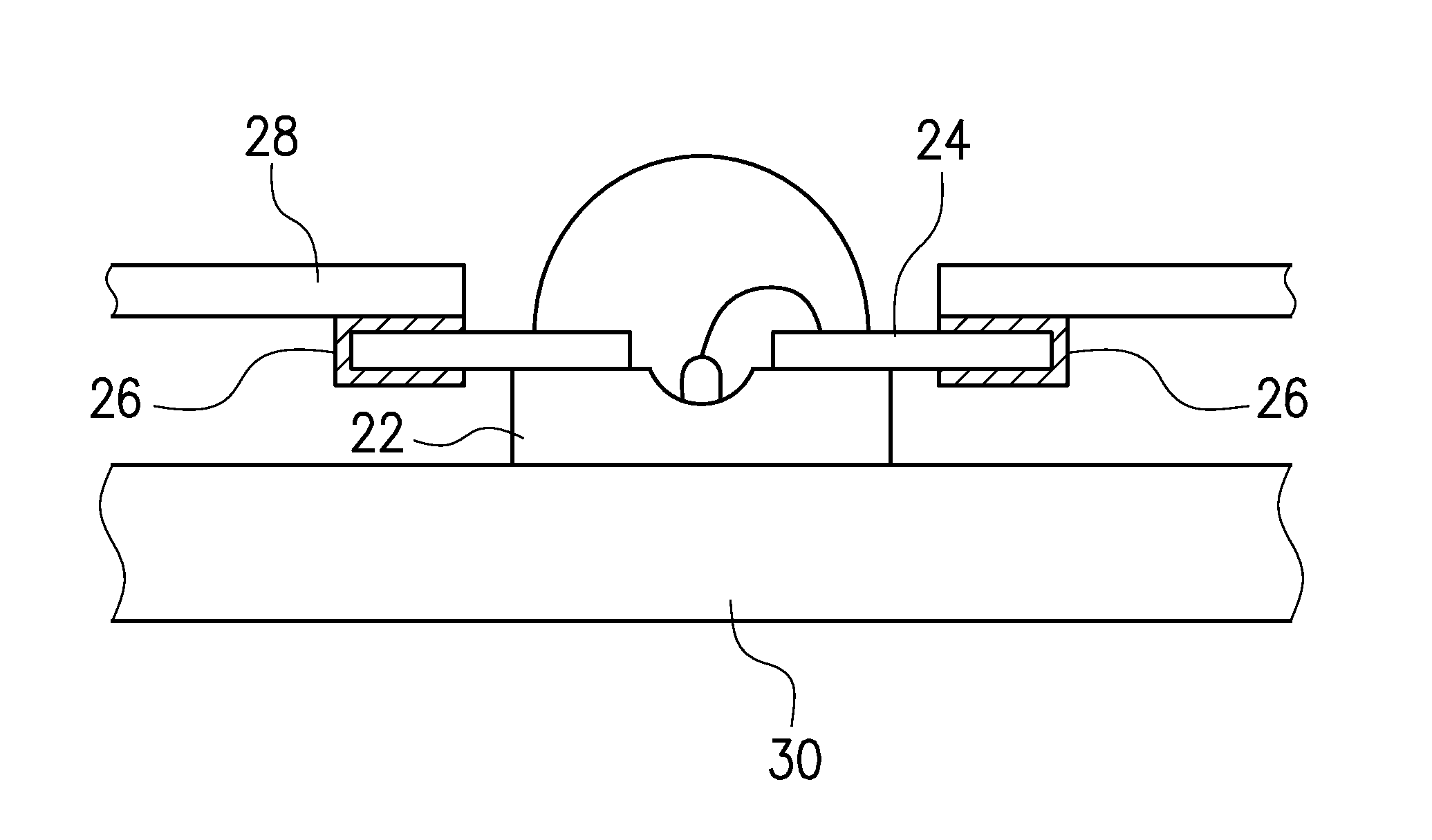
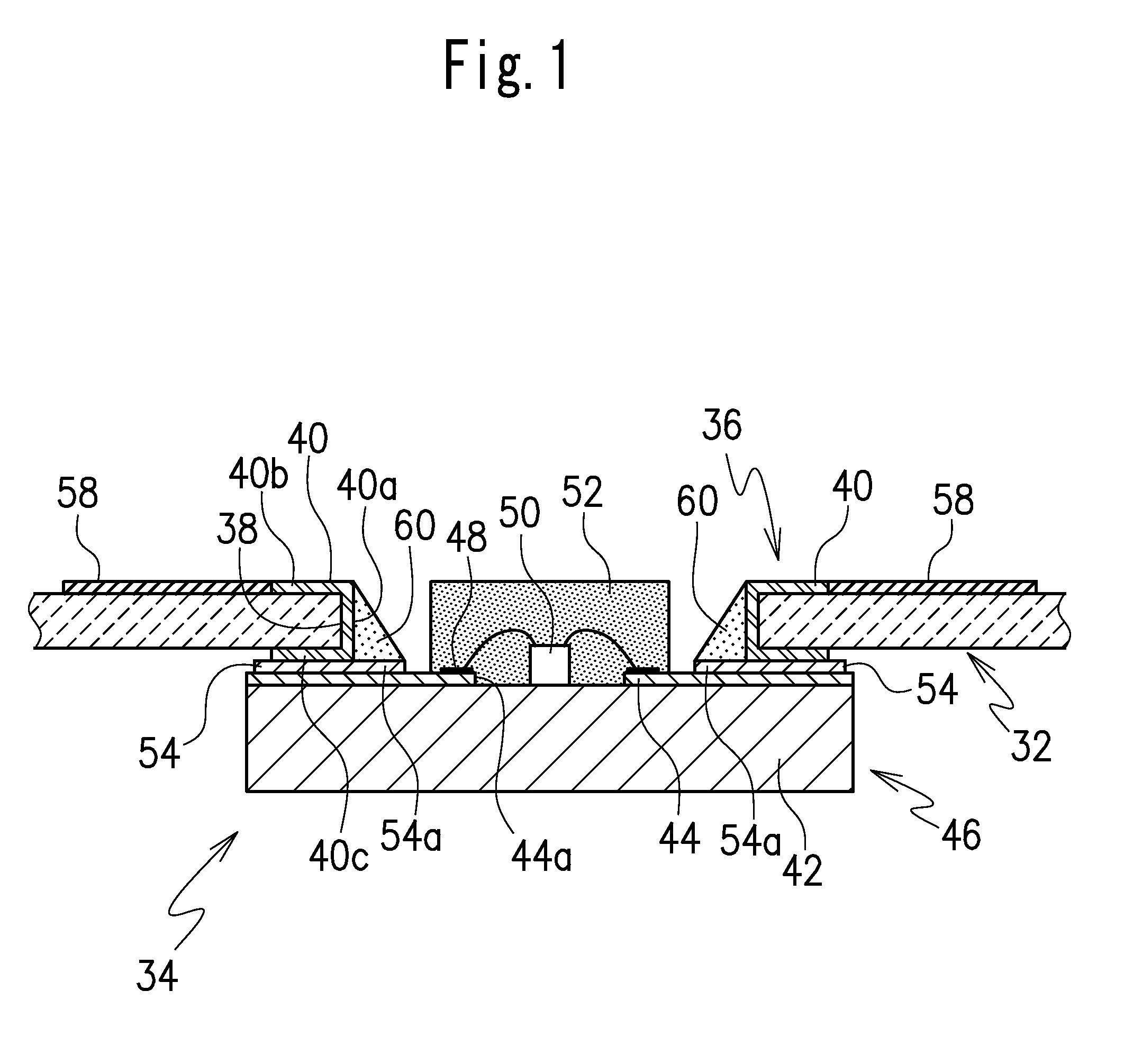
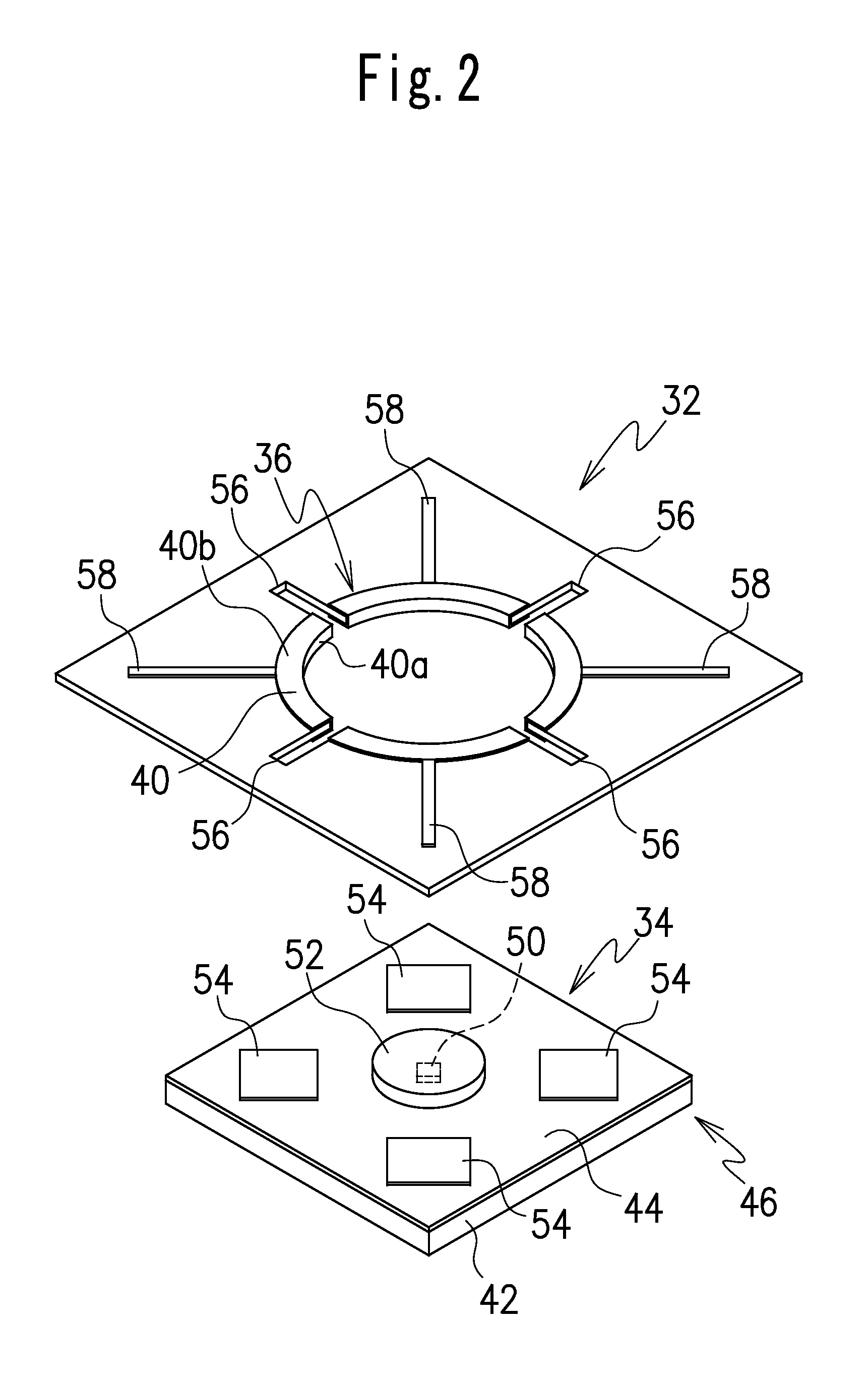
[0033]FIG. 1 is a cross-sectional view showing the upper surface of the substrate of a light-emitting diode, as an electronic component, mounted on the lower surface of a mounting board, according to a first embodiment of the present invention. FIG. 2 is an exploded perspective view illustrating the mounting board and the light-emitting diode. FIG. 3 is a perspective view illustrating the light-emitting diode mounted on the mounting board, and FIG. 4 is an expanded view of portion A of FIG. 3. Reference numeral 32 denotes the mounting board, on the lower surface of which the upper surface of the substrate of the electronic component is mounted. Reference numeral 34 denotes a light-emitting diode as the electronic component. The light-emitting diode 34 according to the present embodiment includes: a substrate 46 having a metal base 42 such as of aluminum and a wiring plate 44, the wiring plate 44 being disposed on the upper surface of the base and having at least one pair of patterne...

second embodiment

[0043]Now, referring to FIGS. 5 to 8, a description will be made to a mounting board 32 of a second embodiment which has a modified pass-through hole 36. Note that in this embodiment, the pass-through hole is partially different in structure from that of the first embodiment, but the other configuration, the material of each portion, the conditions of mounting and the like are the same as those of the first embodiment. Thus, the same portions as those of the first embodiment will be denoted with the same symbols without detailed descriptions. The pass-through hole 36 of the first embodiment was set to have such a diameter that receives therein the light-emitting area of the light-emitting diode and the connecting portion 54a, and had a substantially circular shape in plan view. The connecting portion 54a was at least part of the at least one pair of patterned electrodes 54 provided on the upper surface of the substrate 46 of the light-emitting diode 34 and connected to a plurality o...


PUM


Abstract

A mounting board including a pair of patterned electrodes, a lower surface and an upper surface opposed thereto on which a substrate of an electronic component is to be mounted, a pass-through hole penetrating through the upper surface and the lower surface, and a peripheral side surface that defines the pass-through hole. The pass-through hole includes a plurality of penetrating grooves that are cut into the mounting board and penetrate through the upper and lower surfaces. The plurality of penetrating grooves electrically split the pair of patterned electrodes. The pair of patterned electrodes is partly positioned inside the peripheral side surface, and a connection portion connecting the at least one pair of patterned electrodes and at least one pair of patterned electrodes provided on the upper surface of the substrate of the electronic component is to be disposed inside the peripheral side surface that defines the pass-through hole.

Description

TECHNICAL FIELD[0001]The present invention relates to a mounting board to mount an electronic component such as an IC or a light-emitting diode. More particularly, the invention relates to a mounting board, from a lower surface of which, an electronic component is to be mounted, and a structure of the mounting board on that the electronic component is mounted.BACKGROUND ART[0002]As shown in FIGS. 9 and 10, as an example of an electronic component to be mounted on a mounting board, there is shown a light-emitting diode. The light-emitting diode 2 has a light-emitting element 4, a substrate 6 on which the light-emitting element 4 is mounted, and a pair of patterned electrodes 8 and 10, which are formed to extend from the upper surface to the side surfaces of the substrate 6, or a pair of through hole electrodes 12. Note that the light-emitting element 4 is electrically connected to the pair of patterned electrodes 8 and 10 or the pair of through hole electrodes 12 and then sealed in a...

Claims


Application Information

Patent Timeline
Patent Type & Authority Applications(United States)
IPC IPC(8): H05K1/11H01L33/62
CPCH01L33/62H01L33/64H01L2224/48091H01L2224/48227H01L2924/00014
Inventor KASHITANI, KOHSUKEFUKASAWA, KOICHITAKASHIMA, JUNKIYOZUMI, KATSUYUKI
Owner CITIZEN WATCH CO LTD
Why Eureka
Try Eureka