Imaging Device

a technology of imaging device and image, which is applied in the field of imaging device, can solve the problems of image (or video) interference, picture (or video) interference, and the imaging device contains striped-pattern noise (beat noise), and achieve the effect of reducing the external noise and simple internal configuration

Inactive Publication Date: 2012-12-13
PANASONIC CORP
View PDF6 Cites 10 Cited by
  • Summary
  • Abstract
  • Description
  • Claims
  • Application Information

AI Technical Summary

Benefits of technology

[0016]As described above, according to the imaging device of the present invention, picture (or video) interference caused by external noise can be reduced without causing deterioration of the quality of a taken image even when the device is used in a strong electric field environment, and miniaturization can be achieved through having a simple internal configuration.

Problems solved by technology

When the imaging devices are used under such environments, the imaging devices may be subjected to electromagnetic wave interference.
Such an environment where the imaging devices may be subjected to electromagnetic wave interference is referred to as “a strong electric field environment.” If imaging devices such as digital still cameras and the like are used in a strong electric field environment, there are cases where picture (or video) interference occurs, such that images taken by the imaging devices contain striped-pattern noise (beat noise).
Furthermore, associated with miniaturization of the imaging devices, the amount of external strong-electric-field noise coupled to the imaging elements incorporated in the miniaturized imaging devices increases, such that the picture (or video) interference becomes more prominent.
Causes of such picture (or video) interference include penetration of external electromagnetic waves into video signal lines of the imaging elements, or fluctuation of the ground (“GND”) potential of imaging element flexible cables due to the influence of external electromagnetic waves.
However, with this measure, stress is applied on the imaging elements in the traveling direction of light, and thereby the imaging elements will tilt.
As a result, deterioration of image quality occurs in images taken by the imaging devices, and therefore it has been difficult to introduce the measure in actual products.

Method used


Image

  • Imaging Device
  • Imaging Device
  • Imaging Device

Examples


Embodiment Construction

[0030]One embodiment of the present invention will be described in the following with reference to the drawings.

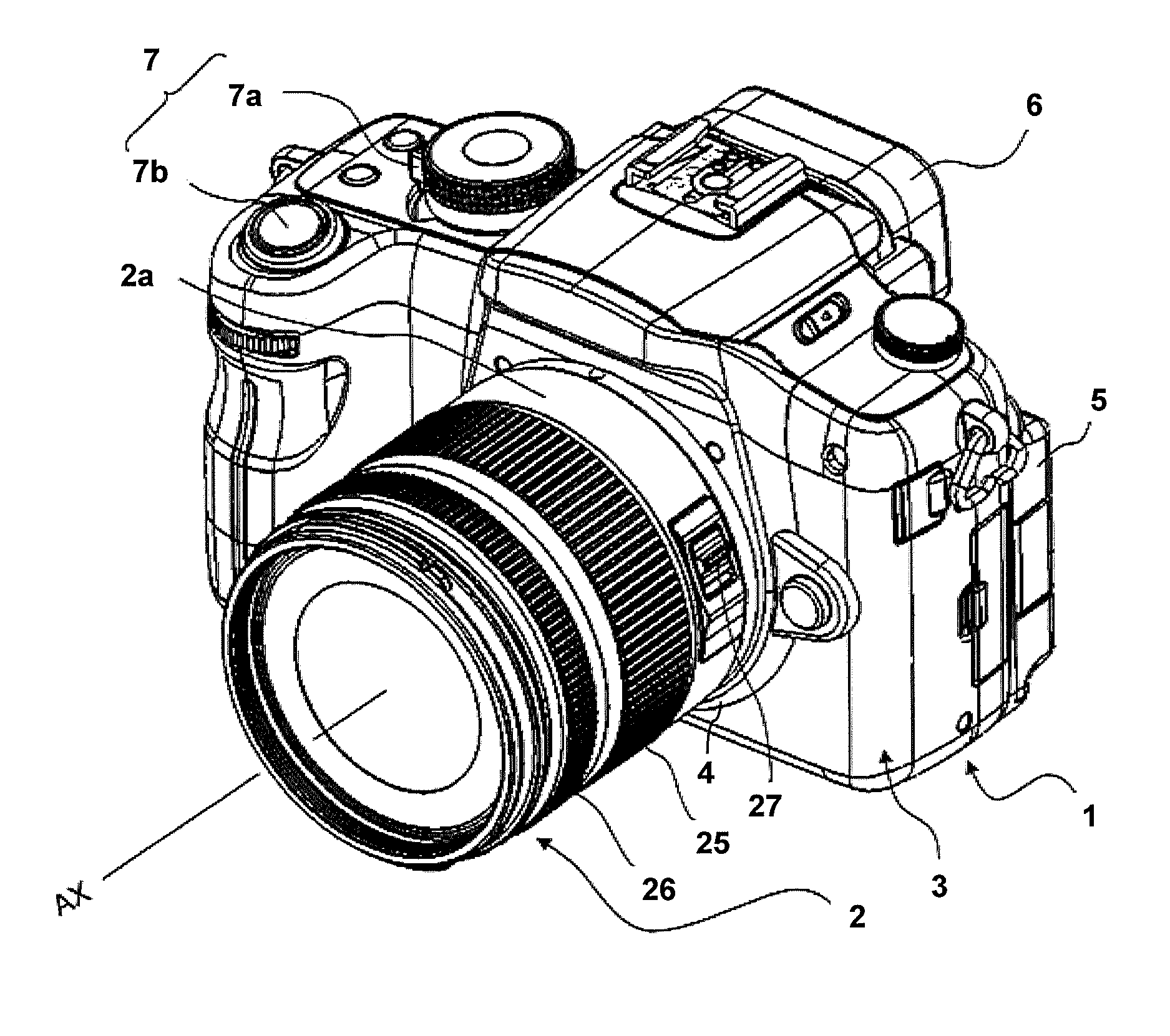
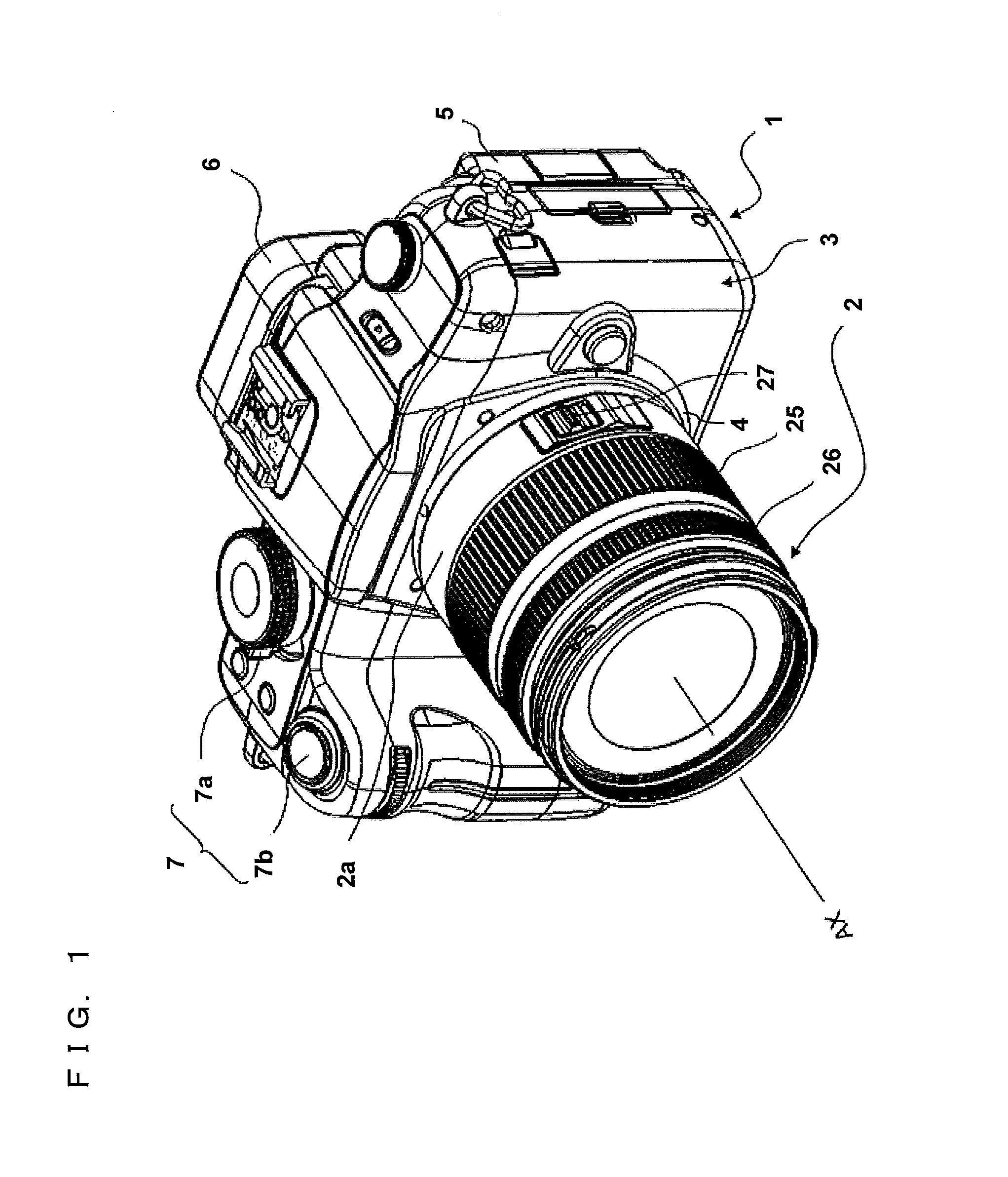
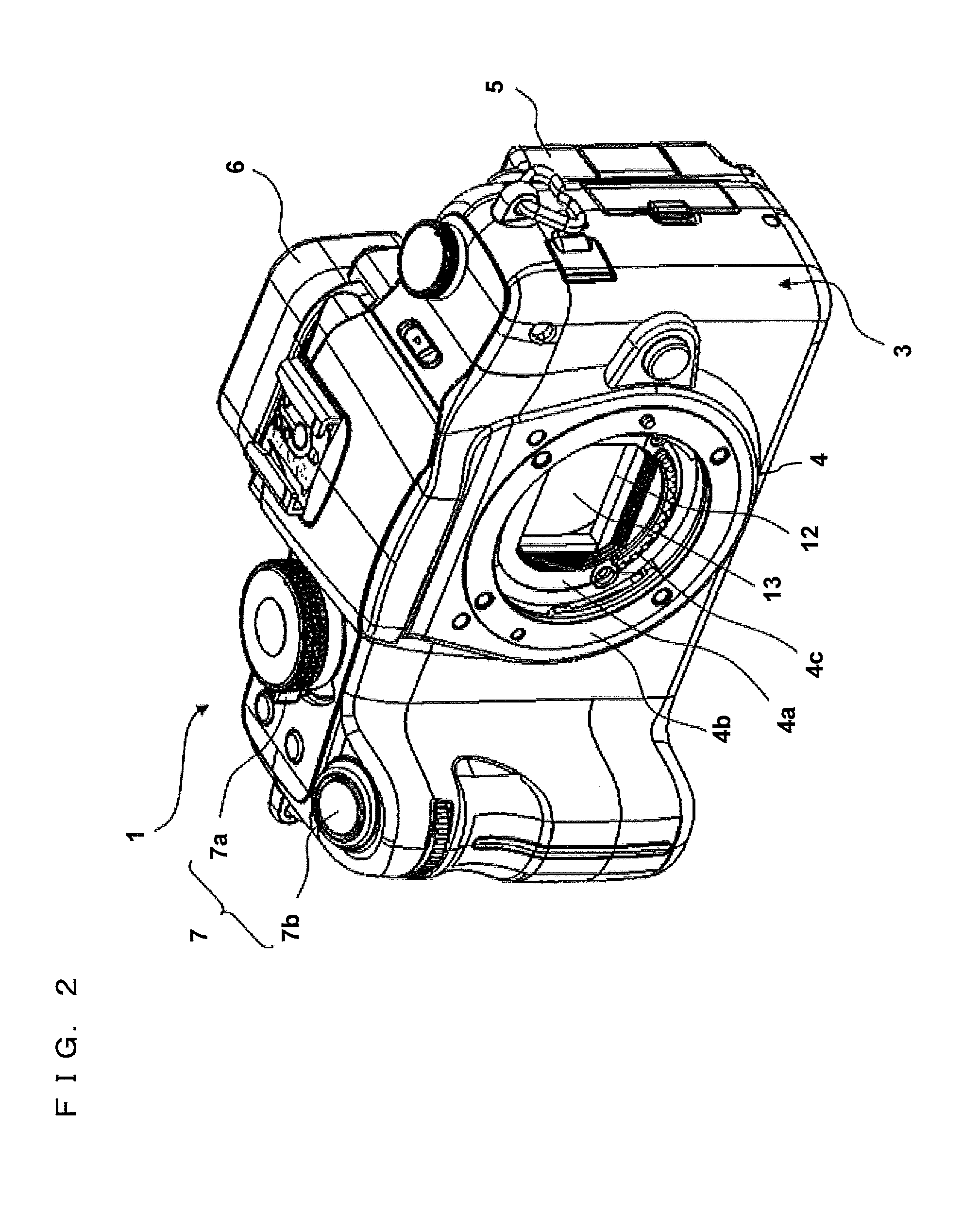
[0031]FIG. 1 is a perspective diagram showing an exterior view of a digital camera (one example of an imaging device) according to one embodiment of the present invention. The digital camera according to one embodiment of the present invention includes a camera body 1 and an interchangeable lens unit 2 that can be mounted on the camera body 1. FIG. 2 is a perspective diagram showing an exterior view of the camera body 1 having removed therefrom the interchangeable lens unit 2. FIG. 3 is an outline cross sectional view of an internal structure of the digital camera. FIG. 4 is a functional block diagram of the digital camera.

[0032]Firstly, the basic configuration of the digital camera according to one embodiment of the present invention will be described with reference to FIG. 1 to FIG. 4. Here, for convenience of description, the photographic-subject side of the digital cam...


PUM


Abstract

An imaging device of the present invention includes: an imaging element for taking an optical image of a photographic subject and generating image data therefrom; a main circuit board for conducting signal processing on the image data, an imaging element flexible cable on which the imaging element is mounted and that has a ground potential; a shutter that opens and closes timed on the shooting of images or video of the photographic subject; a shutter flexible cable that transfers a control signal for controlling the shutter and that has a ground potential; a mount for fixing the imaging element and that includes a metallic component; and a metal plate that is connected to the mount and is disposed between the imaging element and the main circuit board. Therein, the ground potential of the imaging element and the shutter flexible cable are connected.

Description

TECHNICAL FIELD[0001]The present invention relates to imaging devices such as digital still cameras and the like, and more specifically, relates to imaging devices for reducing picture (or video) interference caused by external noise.BACKGROUND ART[0002]In recent years, occasions in which imaging devices such as digital still cameras and the like are employed in environments where electromagnetic wave-radiating handheld information terminals such as mobile phones and PHS's (Personal Handyphone Systems) are used are increasing. In addition, occasions in which imaging devices such as digital still cameras and the like are employed in environments, including the vicinity of radio broadcasting stations and television broadcasting stations, for example, where strong electromagnetic waves are radiated are also increasing.[0003]When the imaging devices are used under such environments, the imaging devices may be subjected to electromagnetic wave interference. Such an environment where the ...

Claims


Application Information

Patent Timeline
Patent Type & Authority Applications(United States)
IPC IPC(8): H04N5/225
CPCG03B9/08G03B17/14G03B2217/002H04N5/2254G03B2206/00H04N5/2253H04N23/54H04N23/55H04N23/60
Inventor TOBINAGA, MASATOFUSAYASU, HIROTSUGUKUMOI, MASAFUMI
Owner PANASONIC CORP
Why Eureka
Try Eureka