Multiple-Bit Programmable Resistive Memory Using Diode as Program Selector

Active Publication Date: 2012-12-13
ATTOPSEMI TECH CO LTD
View PDF6 Cites 124 Cited by
  • Summary
  • Abstract
  • Description
  • Claims
  • Application Information

AI Technical Summary

Benefits of technology

[0018]Embodiments of memory devices are disclosed herein. Certain embodiments disclosed concern programmable resistive device cells using polysilicon diodes as program selectors are disclosed. The programmable resistive devices can be fabricated using standard CMOS logic processes to reduce cell size and cost. In one embodiment, a programmable resistive device and memory can use diodes fabricated on a polysilicon as program selectors, where the P and N terminals of the diode are P+ and N+

Problems solved by technology

As a result, the cell size of an electrical fuse using silicided polysilicon tends to be very large.
Though this technology can reduce the PCM cell size to only 6.8 F2 (F stands for feature size), the diode requires very complicated process steps

Method used


Image

  • Multiple-Bit Programmable Resistive Memory Using Diode as Program Selector
  • Multiple-Bit Programmable Resistive Memory Using Diode as Program Selector
  • Multiple-Bit Programmable Resistive Memory Using Diode as Program Selector

Examples


Embodiment Construction

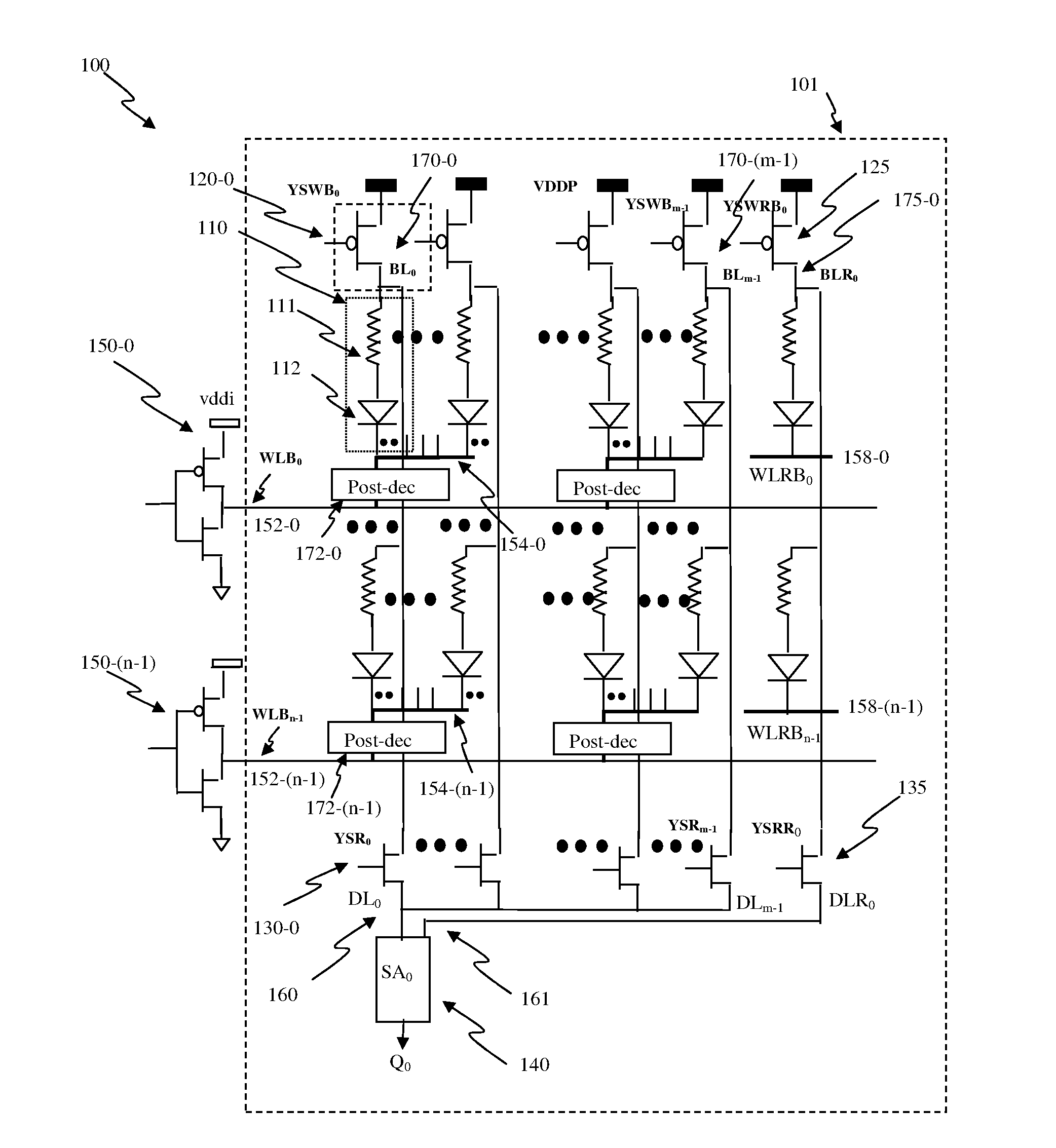
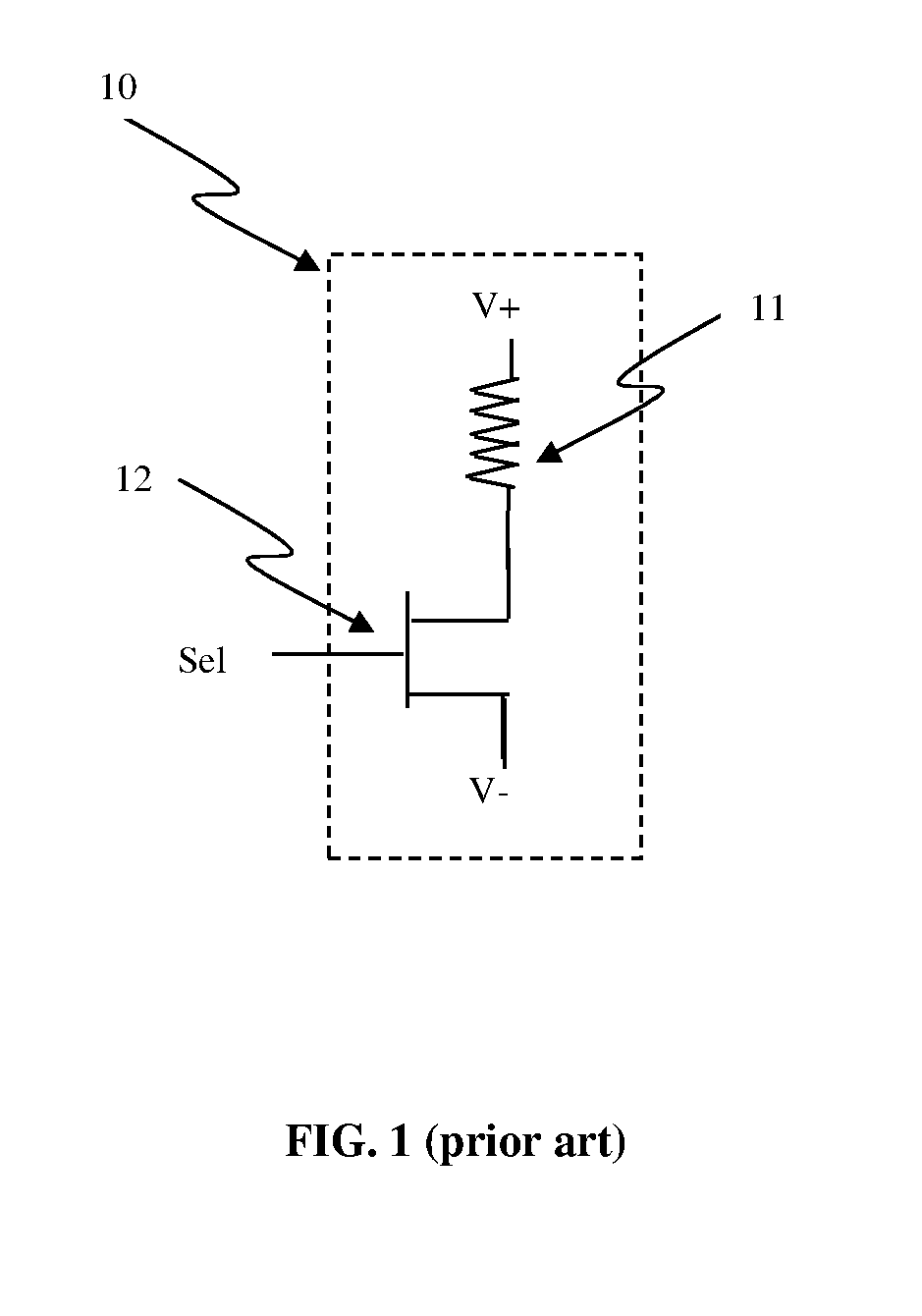
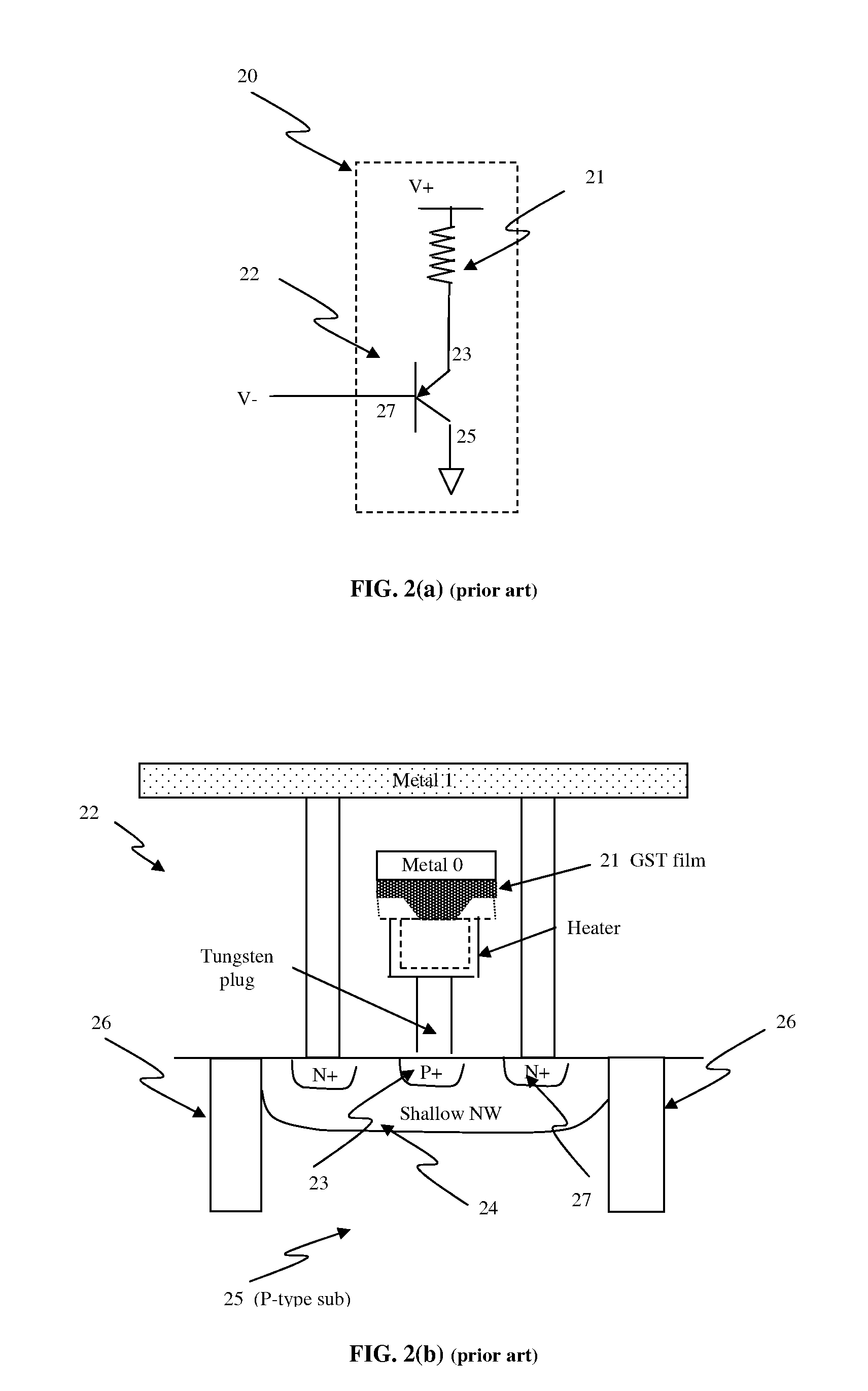
[0080]Embodiments disclosed herein use a polysilicon diode as program selector for a programmable resistive device. The diode can comprise P+ and N+ implants on a polysilicon substrate. Since the P+ and N+ implants and polysilicon are readily available in standard CMOS logic processes, these devices can be formed in an efficient and cost effective manner. There are no additional masks or process steps to save costs. The programmable resistive device can also be included within an electronic system.

[0081]Embodiments of a method and system for multiple-bit programmable resistive cells having a multiple-bit programmable resistive element and using diode as program selector are disclosed. The first and second terminals of the diode having a first and second types of dopants can be fabricated from source / drain of MOS in a well for MOS devices or fabricated on the same polysilicon structure. If a multiple-bit programmable resistive cell has 2n (n>1) distinct resistance levels to store n-b...


PUM


Abstract

A method and system for multiple-bit programmable resistive cells having a multiple-bit programmable resistive element and using diode as program selector are disclosed. The first and second terminals of the diode having a first and second types of dopants can be fabricated from source/drain of MOS in a well for MOS devices or fabricated on the same polysilicon structure. If a multiple-bit programmable resistive cell has 2n (n>1) distinct resistance levels to store n-bit data, at least 2n−1 reference resistance levels can be designated to differential resistances between two adjacent states. Programming multiple-bit programmable resistive elements can start by applying a program pulse with initial program voltage (or current) and duration. A read verification cycle can follow to determine if the desirable resistance level is reached. If the desired resistance level has not been reached, additional program pulses can be applied.

Description

CROSS-REFERENCE TO RELATED APPLICATIONS[0001]This application is a continuation-in-part of U.S. patent application Ser. No. 13 / 026,725, filed on Feb. 14, 2011, and entitled “CIRCUIT AND SYSTEM OF USING A JUNCTION DIODE AS PROGRAM SELECTOR FOR RESISTIVE DEVICES,” which is hereby incorporated herein by reference, and which in turn claims priority benefit of (i) U.S. Provisional Patent Application No. 61 / 375,653, filed on Aug. 20, 2010 and entitled “CIRCUIT AND SYSTEM OF USING JUNCTION DIODE AS PROGRAM SELECTOR FOR RESISTIVE DEVICES IN CMOS LOGIC PROCESSES,” which is hereby incorporated herein by reference; and (ii) U.S. Provisional Patent Application No. 61 / 375,660, filed on Aug. 20, 2010 and entitled “CIRCUIT AND SYSTEM OF USING POLYSILICON DIODE AS PROGRAM SELECTOR FOR RESISTIVE DEVICES IN CMOS LOGIC PROCESSES,” which is hereby incorporated herein by reference.[0002]This application is a continuation-in-part of U.S. patent application Ser. No. 13 / 026,650, filed on Feb. 14, 2011, and...

Claims


Application Information

Patent Timeline
IPC IPC(8): G11C11/21G11C11/02G11C17/16G11C17/06
CPCG11C11/5678G11C2213/74G11C11/5692G11C13/0004G11C13/0007G11C13/003G11C13/0038G11C13/004G11C13/0064G11C13/0069G11C2013/0054G11C2013/0073G11C2013/0092G11C2213/72G11C11/5685
Inventor CHUNG, SHINE C.
Owner ATTOPSEMI TECH CO LTD
Why Eureka
Try Eureka