Check patentability & draft patents in minutes with Patsnap Eureka AI!

Integrated circuit design tool apparatus and method of designing an integrated circuit

a technology of integrated circuit and tool apparatus, which is applied in the direction of error detection/correction, instruments, program control, etc., can solve the problems of unnecessarily waste of silicon “real estate”, time-consuming use of optimiser in conjunction with circuit simulator, and fiscal cost of designing integrated circui

Inactive Publication Date: 2012-12-13
NXP USA INC
View PDF3 Cites 4 Cited by
  • Summary
  • Abstract
  • Description
  • Claims
  • Application Information

AI Technical Summary

Problems solved by technology

However, use of conservatively estimated guard bands results in transistors being formed further from the well edge than is necessary, a consequential result being that silicon “real estate” is unnecessarily wasted.
The use of the Optimiser in conjunction with the circuit simulator is time consuming due to the number of iterations that need to be performed and the large number of parameters that potentially can be altered before an optimum solution can be found.
As will be appreciated by the skilled person, such a solution is computationally complex, and the time consuming nature of the technique, contributes considerably to the fiscal cost of designing the integrated circuit.
However, the system of U.S. Pat. No. 7,089,512 is limited to signal integrity performance and is also an iterative process that is still computationally expensive as explained above.

Method used


Image

  • Integrated circuit design tool apparatus and method of designing an integrated circuit
  • Integrated circuit design tool apparatus and method of designing an integrated circuit
  • Integrated circuit design tool apparatus and method of designing an integrated circuit

Examples


Embodiment Construction

[0018]Because the illustrated embodiments of the present invention may for the most part, be implemented using electronic components and circuits known to those skilled in the art, details will not be explained in any greater extent than that considered necessary as illustrated above, for the understanding and appreciation of the underlying concepts of the present invention and in order not to obfuscate or distract from the teachings of the present invention.

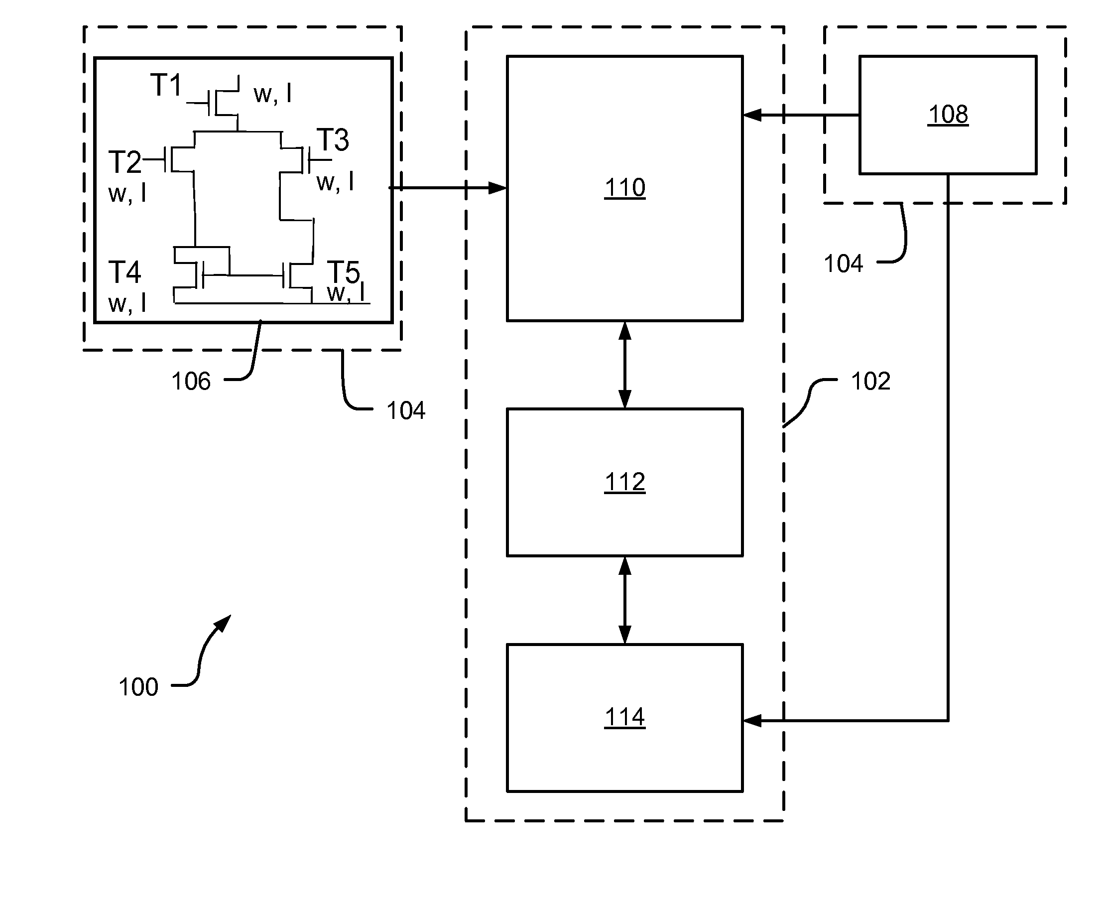
[0019]Referring now to FIG. 1, an integrated circuit design tool apparatus 100 comprises a processing resource, for example a processor 102 of a Personal Computer (PC) or other computing apparatus and a storage device, for example a memory of the PC, such as a digital memory 104, for storing integrated circuit design data 106. In this example, the design data 106 comprises electrical schematic data defining, for example, interconnections between devices, such as MOSFETS, capacitors and resistors, and layout data, for example inf...


PUM


Abstract

An integrated circuit design tool apparatus including a processing resource arranged to support a circuit simulator, a circuit simulator interrogator, and a well distance calculator is provided. The circuit simulator interrogator communicates first and second well distance values separately to the circuit simulator and receives first and second performance parameter value back from the circuit simulator interrogator in response. The well distance calculator determines a performance parameter limit value, and projects, substantially linearly, a well distance change value in respect of the performance parameter limit value using the first and second performance parameter values, the performance parameter limit value and a trial well distance change value. Also, a well distance change characterising equation using the well distance change value projected is used in order to obtain the minimum well distance value associated with the performance parameter limit value.

Description

FIELD OF THE INVENTION[0001]This invention relates to an integrated circuit design tool apparatus of the type that, for example, minimises a well distance in respect of a semiconductor device. This invention also relates to a method of designing an integrated circuit, the method being of the type that, for example, minimises a well distance in respect of a semiconductor device design.BACKGROUND OF THE INVENTION[0002]In the field of semiconductor device design, it is well known to fabricate switching devices, for example, transistors, on silicon (Si) or other semiconductor materials. It is also known to form wells in the silicon by implanting ions of another element. Indeed, so called high energy ion implanters are known for forming relatively heavily doped n-wells and p-wells. It is also known to form deep buried wells using ion implanters.[0003]Typically, the implanted regions are formed in a well-known manner by depositing photoresist on a surface of a semiconductor material, the ...

Claims


Application Information

Patent Timeline
Patent Type & Authority Applications(United States)
IPC IPC(8): G06F17/50
CPCG06F17/5072G06F30/392
Inventor CAUNEGRE, PASCAL
Owner NXP USA INC
Features
  • R&D
  • Intellectual Property
  • Life Sciences
  • Materials
  • Tech Scout
  • Unparalleled Data Quality
  • Higher Quality Content
  • 60% Fewer Hallucinations
Learn More