Optical Sensor, in Particular Proximity Switch

Active Publication Date: 2013-01-03
SIEMENS HEALTHCARE GMBH
View PDF2 Cites 4 Cited by
  • Summary
  • Abstract
  • Description
  • Claims
  • Application Information

AI Technical Summary

Benefits of technology

[0013]The presently disclosed embodiment provides a wealth of advantages. A beam subdivision is performed in the optical sensor in accordance with the invention using optical elements that are distributed in an appropriate manner. As a result, the transmission light beam has a considerably higher transmission power, with the result that the optical transmitting unit for generating the beam can have smaller dimensions. The photosensitive area detector provides a common detector area both for the light emanating from the sensor and for the light incident in the sensor. As a result, common or conventional optics are sufficient.
[0014]A particular advantage of this arrangement is that, on account of the fact that both light levels are measured using the same photosensitive area detector, these light levels can be directly correlated with one another without previous correction factors in evaluation operations. Furthermore, there is no need for any synchronization between the drive device for the transmitting unit and the evaluation unit at the output of the area detector because the temporal transmission information is contained in the single transmission and reflection light beam traveling back and forth. Therefore, only a single evaluation unit is re

Problems solved by technology

If reflection light radiation is received outside these periods of time, this may only be undesirable extraneous light radiation.
The optical elements needed to subdivide the transmissio

Method used


Image

  • Optical Sensor, in Particular Proximity Switch
  • Optical Sensor, in Particular Proximity Switch
  • Optical Sensor, in Particular Proximity Switch

Examples


Embodiment Construction

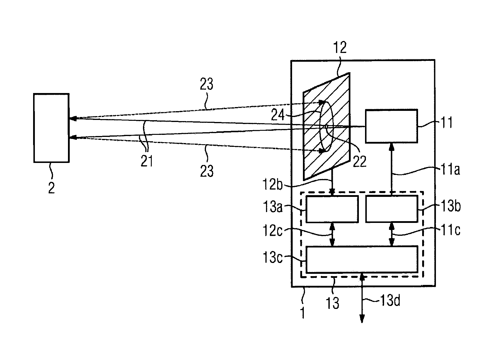
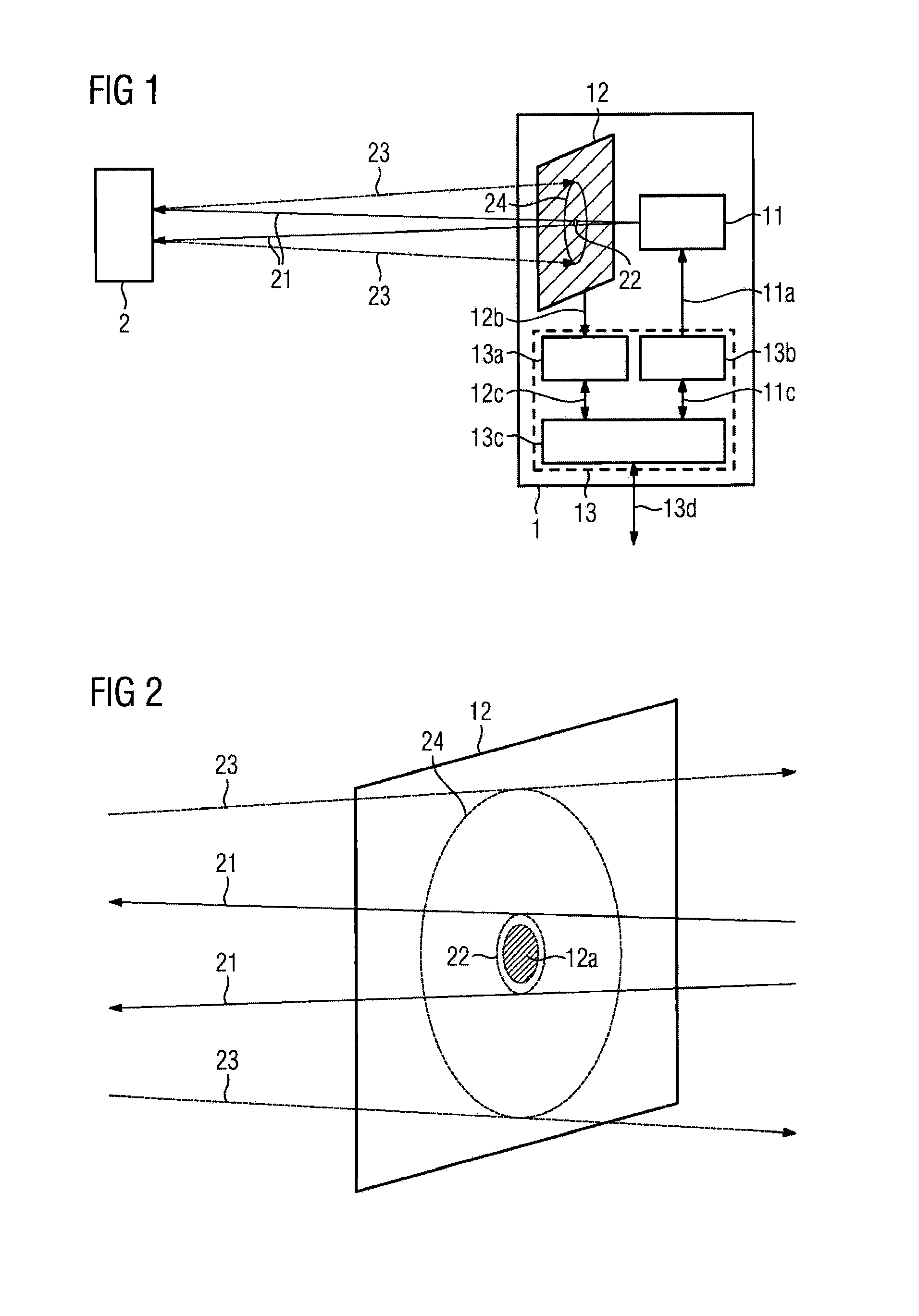
[0023]FIG. 1 shows a block diagram of the schematic structure of an exemplary optical sensor 1 in accordance with the invention. The sensor comprises an individual sensor 1 with an approximately punctiform monitoring region. Here, the sensor 1 contains a photosensitive area detector 12 which has semitransparent properties and is irradiated, virtually from the rear, by an optical transmitting unit 11 with a transmission light beam 21.

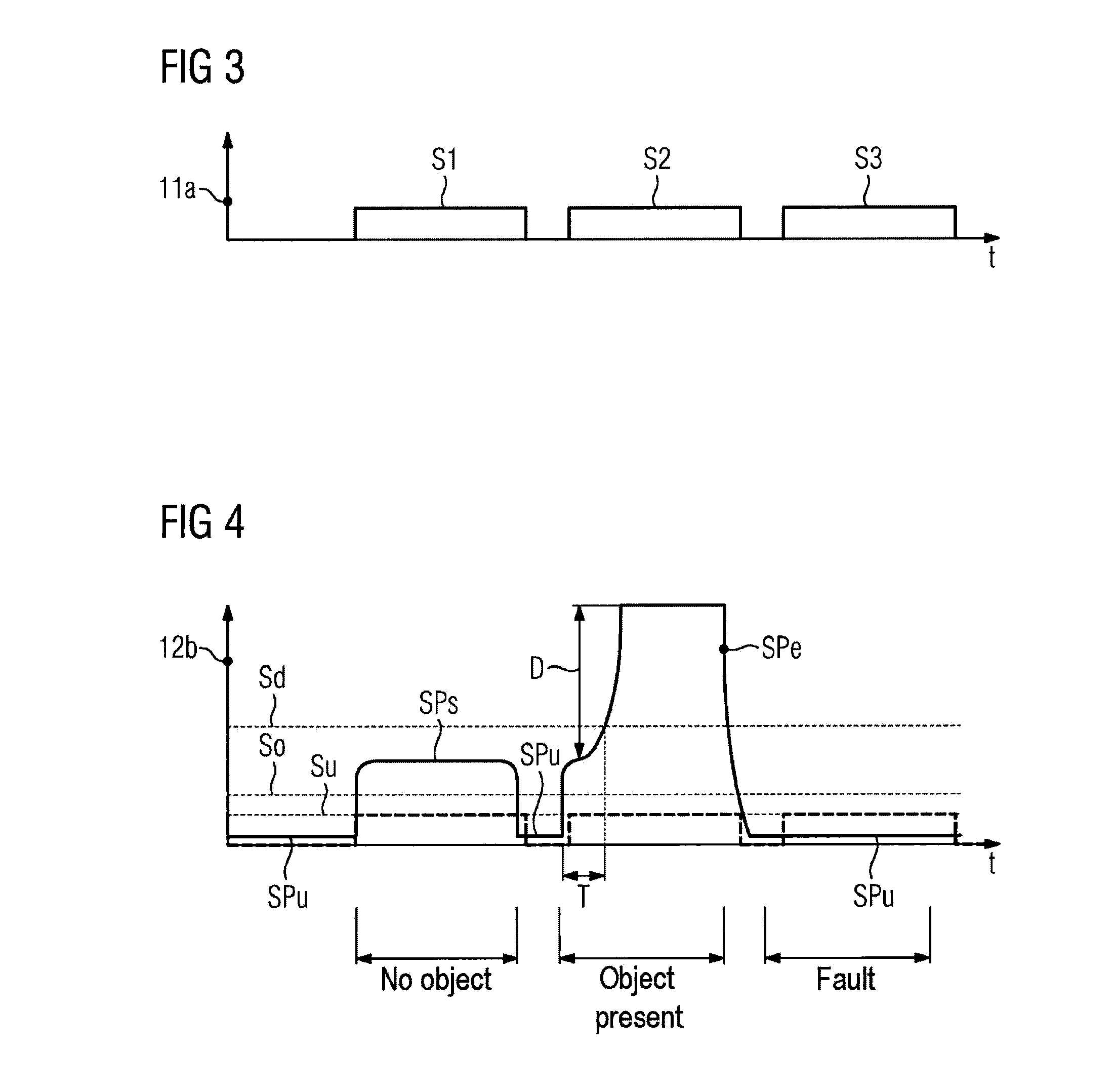
[0024]This transmission light beam 21 is aimed, in the manner of a measuring light beam, at an object to be detected, at a box 2 in the example in FIG. 1, and causes a transmission light spot 22 on the surface of the photosensitive area detector 12. This light spot is detected by the area detector 12 and is passed, as an actual value of the photoelectric current of the area detector 12, to a controller 13 for further processing via an analog measured value output 12b. The controller can use this measured value to detect, for example, the presence of the ...


PUM


Abstract

An optical sensor having at least one optical transmitting unit for production of a transmitted light beam, a photosensitive flat detector with semitransparent characteristics, through which the transmitted light beam passes, and which re-receives reflection light beams, i.e., from an object, and an evaluation unit for the photoelectric current of the photosensitive flat detector, at least for detection of an object. The photosensitive flat detector advantageously includes an organic polymer layer comprising a photosensitive substrate. An “Organic Photosensitive Diode” (OPD) is particularly advantageously used as the photosensitive flat detector with semitransparent characteristics.

Description

CROSS-REFERENCE TO RELATED APPLICATIONS[0001]This is a U.S. national stage of application No. PCT / EP2010 / 063847 filed 21 Sep. 2010. Priority is claimed on German Application No. 10 2009 042 609.4 filed 23 Sep. 2009, the content of which is incorporated herein by reference in its entirety.BACKGROUND OF THE INVENTION[0002]1. Field of the Invention[0003]The invention relates to sensors and, more particularly, to an optical sensor.[0004]2. Description of the Related Art[0005]It is known to use an optical sensor, for example, as a proximity switch, a light barrier or in a light grid, a light curtain or a laser scanner.[0006]High demands in terms of accuracy are imposed on such a sensor. In order to meet these demands, it is conventional practice to subdivide the transmission light beam inside an optical sensor into a measuring light beam and a reference light beam using optics, i.e., prisms or a semitransparent mirror. Whereas the measuring light beam is emitted into a detection area and...

Claims


Application Information

Patent Timeline
IPC IPC(8): H01L31/09G01S17/04
CPCG01S17/026G01V8/14H03K17/941H01L51/00H01L31/00H01L31/0352H03K2217/94108G01S17/04G01S17/02H03K17/94H10K99/00
Inventor VOLKEL, THOMAS
Owner SIEMENS HEALTHCARE GMBH
Why Eureka
Try Eureka