Polarizing element, liquid crystal device, and electronic apparatus
- Summary
- Abstract
- Description
- Claims
- Application Information
AI Technical Summary
Benefits of technology
Problems solved by technology
Method used
Image

Examples
first embodiment
[0051]Hereinafter, a first embodiment of the invention will be described.
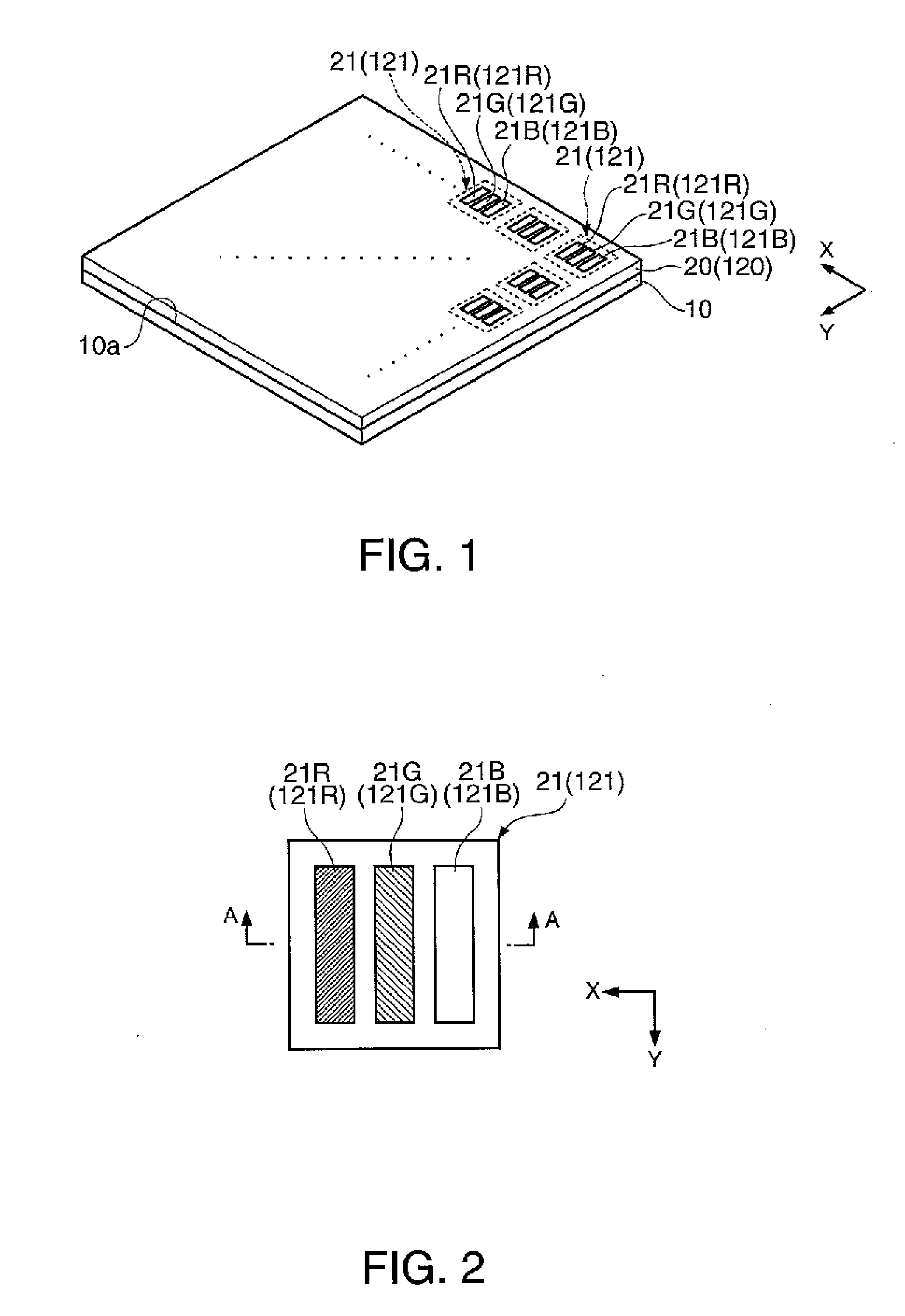
[0052]FIG. 1 is a perspective view showing a polarizing element 20 according to a first embodiment. In the following drawings, the scale of each constituent member is sometimes modified as appropriate for illustrating the constituent member at a recognizable size.
[0053]As shown in FIG. 1, the polarizing element 20 is supported by a glass substrate 10 serving as a backing material. The polarizing element 20 is used by being bonded to, for example, a display surface or the like of a liquid crystal panel having a plurality of pixels made up of a plurality of subpixels.
[0054]A specific material of the glass substrate 10 is not particularly limited, and any known glass substrate maybe used. Incidentally, the material of the glass substrate 10 is not particularly limited to a glass substrate as long as it is a substrate having light transmittance, and a quartz substrate, a rock crystal substrate, a sapphire substrate...
second embodiment
[0087]With reference to FIG. 8, a polarizing element 120 according to a second embodiment of the invention will be described. Incidentally, a point different between the polarizing element 120 according to this embodiment and the polarizing element 20 according to the first embodiment is that each of a polarizing sections 121R, 121G, and 121B provided for the polarizing element 120 contains a light absorbing material, and therefore, the different point will be mainly described. Further, the drawings used for describing the first embodiment will be referred to as appropriate.
[0088]As shown in FIG. 1, the polarizing element 120 is supported by a glass substrate 10 serving as a backing material. The polarizing element 120 is used by being bonded to, for example, a display surface or the like of a liquid crystal panel having a plurality of pixels made up of a plurality of subpixels.
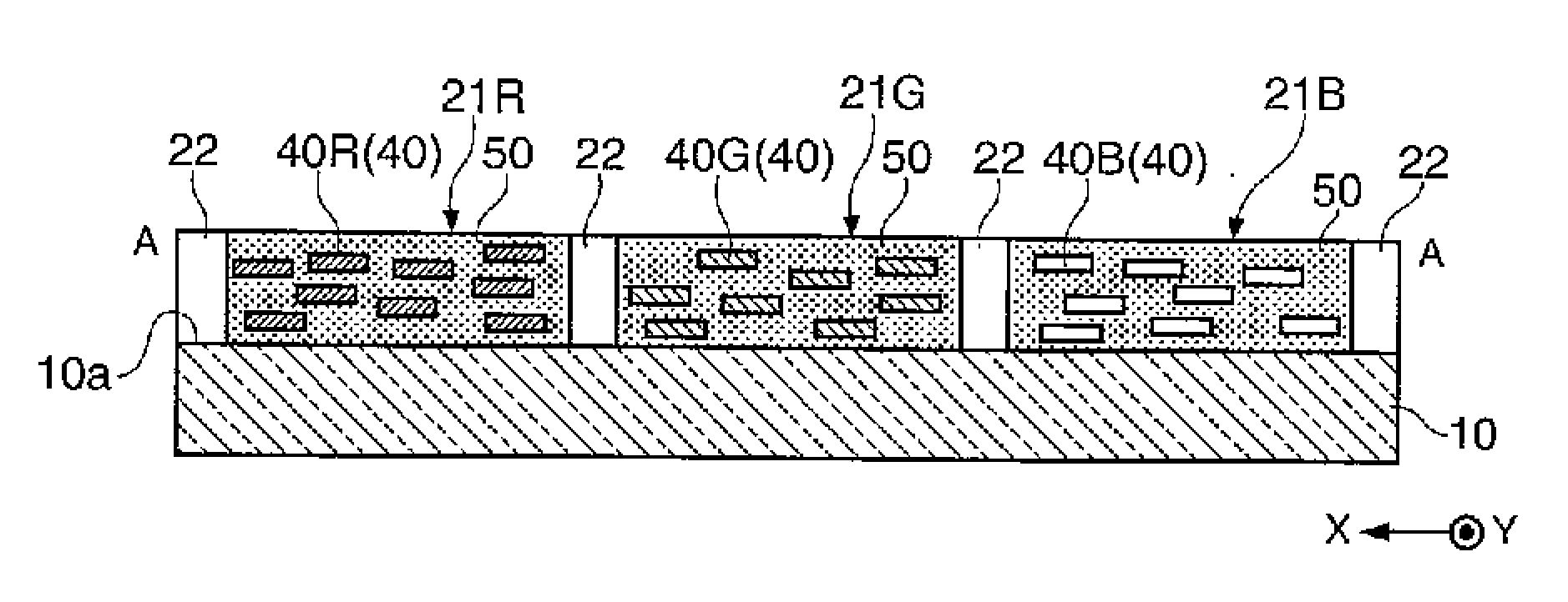
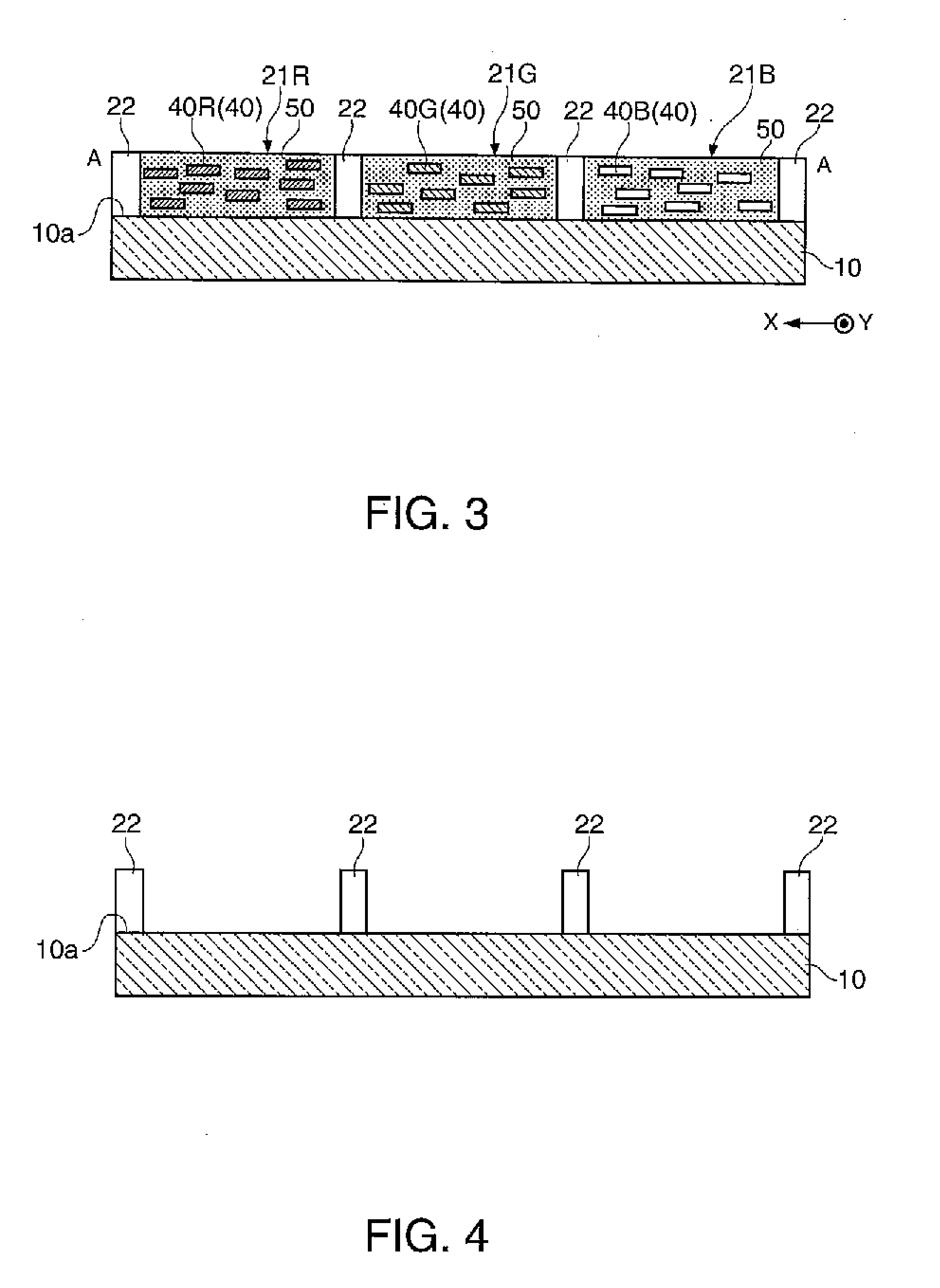
[0089]FIG. 8 is a cross-sectional view taken along the line A-A in FIG. 2.
[0090]As shown in FIG. 8, the po...
third embodiment
[0122]Subsequently, a third embodiment of the invention will be described.
[0123]FIGS. 11 and 12 are views showing a structure of a liquid crystal device according to a third embodiment. In this embodiment, an active matrix type liquid crystal display device using a thin-film transistor (hereinafter abbreviated as “TFT”) as a pixel switching element is described by way of example. FIG. 11 is a plan view of a liquid crystal display device according to this embodiment together with each constituent member seen from a counter substrate side, and FIG. 12 is a cross-sectional view taken along the line H-H′ in FIG. 11.
[0124]As shown in FIGS. 11 and 12, a liquid crystal display device 31 according to this embodiment is provided with a liquid crystal panel 36 in which a TFT array substrate PX and a counter substrate 33 are bonded to each other with a sealing material 34, and a liquid crystal layer 35 is enclosed in a region defined by the sealing material 34. The liquid crystal layer 35 is m...
PUM
 Abstract
Description
Claims
Application Information
 - Generate Ideas
- Intellectual Property
- Life Sciences
- Materials
- Tech Scout
- Unparalleled Data Quality
- Higher Quality Content
- 60% Fewer Hallucinations
Browse by: Latest US Patents, China's latest patents, Technical Efficacy Thesaurus, Application Domain, Technology Topic, Popular Technical Reports.
© 2025 PatSnap. All rights reserved.Legal|Privacy policy|Modern Slavery Act Transparency Statement|Sitemap|About US| Contact US: help@patsnap.com