Shift register

a technology of shift register and shift register, applied in the field of shift register, can solve the problem of unstable low-level potential of output signal ou

Active Publication Date: 2013-01-31
SHARP KK
View PDF11 Cites 31 Cited by
  • Summary
  • Abstract
  • Description
  • Claims
  • Application Information

AI Technical Summary

Benefits of technology

[0022]According to the first aspect of the present invention, to the control terminal of the output transistor is provided a signal for stabilizing the off-potential at the control terminal, through the capacitor. By this, even when the control terminal potential of the output transistor changes with a change in a clock signal, a signal that cancels out the change is provided through the capacitor, enabling to stabilize the control terminal potential of the output transistor. In addition, by using the capacitor when providing the signal to the control terminal of the output transistor, the capability to stabilize the control terminal potential of the output transistor can be maintained even after a lapse of a long time.
[0023]According to the second aspect of the present invention, a signal that changes in an opposite direction to that of the clock signal provided to the output transistor is provided to the control terminal of the output transistor through the capacitor. By this, even when the control terminal potential of the output transistor changes with a change in a clock signal, a signal that cancels out the change is provided through the capacitor, enabling to stabilize the control terminal potential of the output transistor.
[0024]According to the third aspect of the present invention, by using a compensation circuit that provides an opposite-phase clock signal and an off-potential in a switching manner according to the control terminal potential of the output transistor, an output signal can be properly outputted when the control terminal potential is an on-potential, and the control terminal potential can be stabilized at an off-potential when the control terminal potential is an off-potential.
[0025]According to the fourth aspect of the present invention, a compensation circuit that provides an opposite-phase clock signal and an off-potential in a switching manner according to the control terminal potential of the output transistor can be formed using three transistors.
[0026]According to the fifth aspect of the present invention, by providing a fourth transistor, a change in the control terminal potential of the output transistor associated with a change in an output signal can be prevented.
[0027]According to the sixth aspect of the present invention, by providing a capacitor having a capacitance comparable to that of a parasitic capacitance between the first conduction terminal and control terminal of the output transistor, a change in the control terminal potential of the output transistor associated with a change in a clock signal can be effectively prevented.

Problems solved by technology

Hence, leakage current of the output transistor Qo increases and thus the low-level potential of an output signal OUT becomes unstable.

Method used


Image

  • Shift register
  • Shift register
  • Shift register

Examples


first embodiment

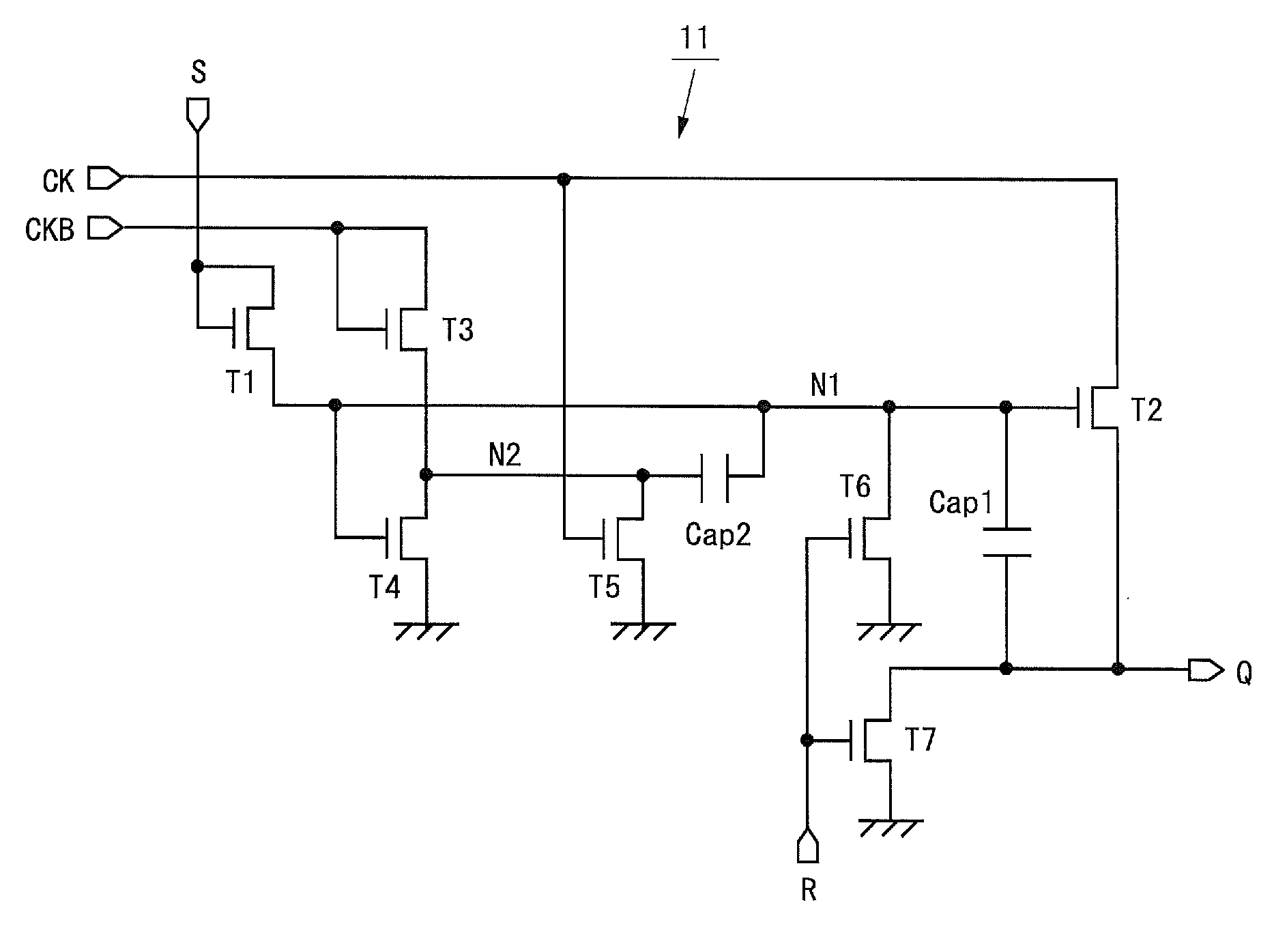
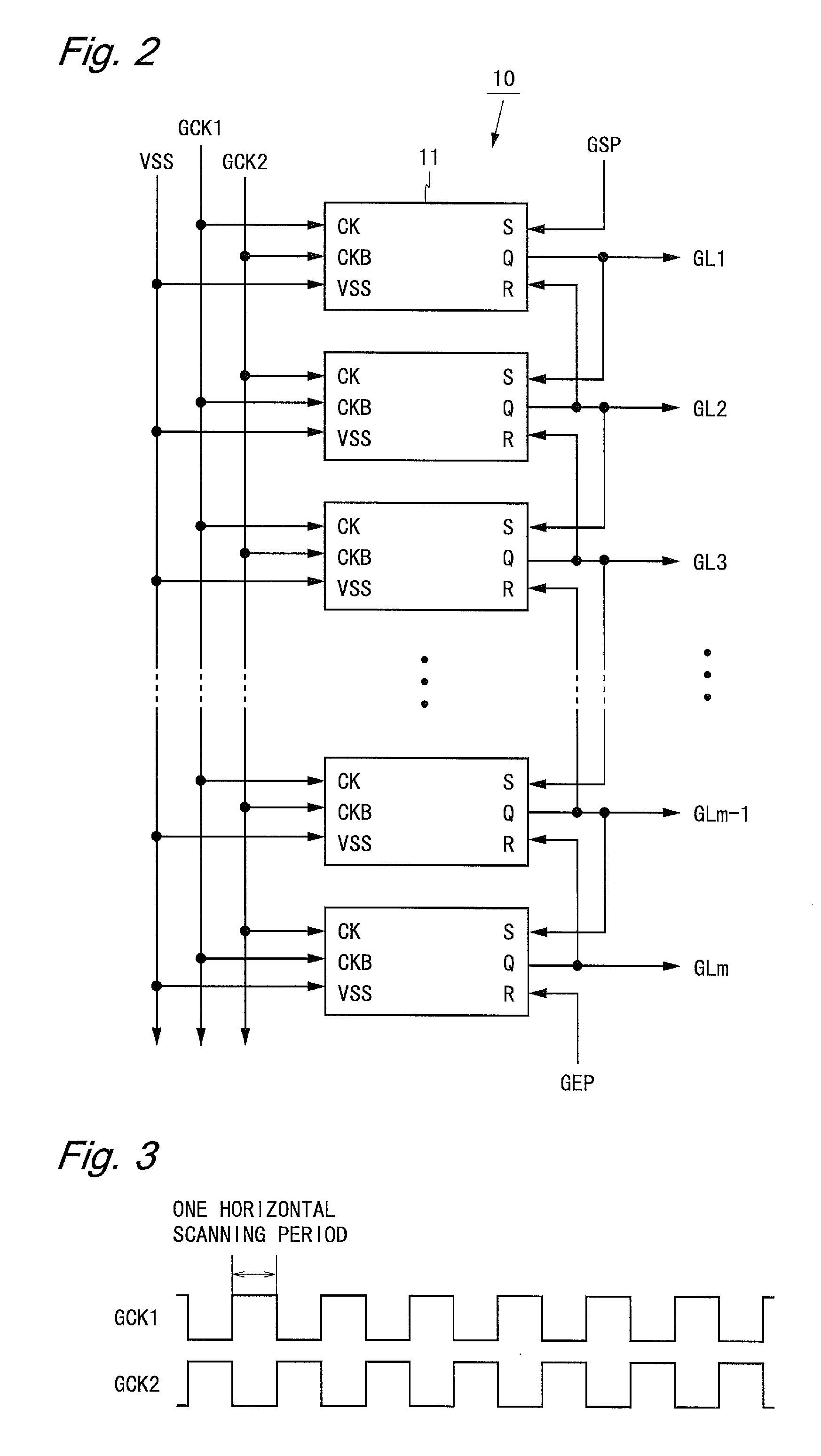
[0058]FIG. 2 is a block diagram showing a configuration of a shift register according to a first embodiment of the present invention. A shift register 10 shown in FIG. 2 includes m unit circuits 11 arranged side by side one-dimensionally. A unit circuit 11 which is arranged in an i-th position (i is an integer between 1 and m, inclusive) is hereinafter referred to as an i-th unit circuit.

[0059]Two gate clock signals GCK1 and GCK2 are supplied to the shift register 10 as gate clock signals GCK. In addition, a gate start pulse signal GSP, a gate end pulse signal GEP, and a low-level potential VSS are supplied to the shift register 10. FIG. 3 is a timing chart of the gate clock signals GCK1 and GCK2. As shown in FIG. 3, the gate clock signal GCK2 is a clock signal of opposite phase to the gate clock signal GCK1. The cycle of the gate clock signals GCK1 and GCK2 is two horizontal scanning periods.

[0060]Clock signals CK and CKB, a set signal S, a reset signal R, and a low-level potential...

second embodiment

[0077]A shift register according to a second embodiment of the present invention has the same configuration (FIG. 2) as the shift register according to the first embodiment and includes unit circuits different than those of the shift register according to the first embodiment. Differences between the present embodiment and the first embodiment will be described below.

[0078]FIG. 8 is a circuit diagram of a unit circuit included in a shift register according to the present embodiment. A unit circuit 21 shown in FIG. 8 is such that a transistor T8 is added to the unit circuit 11 according to the first embodiment (FIG. 4). The drain terminal of the transistor T8 is connected to the node N1 and the gate terminal is connected to the node N2. The low-level potential VSS is fixedly applied to the source terminal of the transistor T8. The transistor T8 applies the low-level potential to the node N1 when the potential at the node N2 is at high level.

[0079]FIG. 9 is a diagram showing a part of...

third embodiment

[0083]FIG. 11 is a block diagram showing a configuration of a shift register according to a third embodiment of the present invention. A shift register 30 shown in FIG. 11 includes m unit circuits 31 arranged side by side one-dimensionally. Differences between the present embodiment and the first embodiment will be described below.

[0084]A clock signal CK, a set signal S, a reset signal R, and a low-level potential VSS are inputted to each unit circuit 31 and an output signal Q is outputted from each unit circuit 31. A gate clock signal GCK1 is inputted to the odd-numbered unit circuits as the clock signal CK. A gate clock signal GCK2 is inputted to the even-numbered unit circuits as the clock signal CK.

[0085]FIG. 12 is a circuit diagram of the unit circuit 31. The unit circuit 31 shown in FIG. 12 is such that the transistors T3 to T5 and the capacitor Cap2 are removed from the unit circuit 11 according to the first embodiment (FIG. 4) and a capacitor Cap3 is added. One electrode of ...


PUM


Abstract

A shift register is formed by connecting unit circuits 11 in multi-stage. One electrode of a capacitor Cap2 in the unit circuit 11 is connected to the gate terminal (node N1) of a transistor T2, and the other connected to a node N2. A compensation circuit composed of transistors T3 to T5 provides a clock signal CKB to the node N2 when the node N1 potential is at low level, and applies a low-level potential to the node N2 when the node N1 potential is at high level. Accordingly, even when the gate potential of the transistor T2 changes with a change in a clock signal CK, a signal that cancels out the change is provided through the capacitor Cap2, stabilizing the gate potential of the transistor T2. Thus, a change in the control terminal potential of an output transistor associated with a change in a clock signal is prevented.

Description

TECHNICAL FIELD[0001]The present invention relates to a shift register and more particularly to a shift register to be favorably used in a drive circuit of a display device, or the like.BACKGROUND ART[0002]An active matrix-type display device displays an image by selecting two-dimensionally arranged pixel circuits on a row-by-row basis and writing grayscale voltages according to a video signal to the selected pixel circuits. Such a display device is provided with a scanning signal line drive circuit including a shift register, to select pixel circuits on a row-by-row basis.[0003]For a method of making a display device small, there is known a method in which a scanning signal line drive circuit is integrally formed with pixel circuits on a display panel, using a fabrication process for forming TFTs (Thin Film Transistors) in the pixel circuits. The scanning signal line drive circuit is formed using, for example, amorphous silicon TFTs. A display panel having an integrally formed scan...

Claims


Application Information

Patent Timeline
Patent Type & Authority Applications(United States)
IPC IPC(8): G11C19/28
CPCG09G3/3677G09G2310/0267G11C19/28G11C19/184G09G2310/0286
Inventor KIKUCHI, TETSUOTANAKA, SHINYASHIMADA, JUNYAYAMASAKI, CHIKAO
Owner SHARP KK
Why Eureka
Try Eureka