Semiconductor integrated circuit having a surface-emitting laser, manufacturing method of the same, and electronic equipment

a technology of integrated circuits and lasers, which is applied in the direction of lasers, semiconductor laser structural details, and semiconductor lasers. it is difficult to accurately monitor the amount of light emitted by the surface-emitting laser for a long period of time, and the gap between the surface-emitting laser and the light receiving device is created

Inactive Publication Date: 2004-09-23
SEIKO EPSON CORP
View PDF6 Cites 36 Cited by
  • Summary
  • Abstract
  • Description
  • Claims
  • Application Information

AI Technical Summary

Benefits of technology

[0009] According to an aspect of the invention, the surface-emitting laser including the micro tile-like element emits laser light in two directions. Laser light in one direction is emitted from the back surface side of the surface-emitting laser, passes through the transparent substrate, and goes out as front light. Laser light in the other direction is emitted from the surface side of the surface-emitting laser and enters the light receiving device. Thus, an aspect of the invention makes it possible to monitor the output of the surface-emitting laser. Since the integrated circuit chip is arranged so as to cover the surface-emitting laser, the integrated circuit chip blocks ambient light incident on the light receiving device. This makes it possible to precisely monitor the output of the surface-emitting laser.
[0054] Thus, it is possible to converge, diverge, change a path of, and divide light emitted from the surface-emitting laser. Therefore, it is possible to easily manufacture various electronic equipment that are significantly compact in size with the semiconductor integrated circuit of an aspect of the invention.

Problems solved by technology

Unlike edge emitting lasers, it is difficult to utilize rear light for surface-emitting lasers because light is emitted from a semiconductor surface.
However, the above-mentioned related art method to monitor the amount of light emitted by a surface-emitting laser involves the following problems.
Moreover, since the amount of reflected light L20 may vary due to dirt on, or deformation of, the glass surface 52, it is difficult to accurately monitor the amount of light emitted by a surface-emitting laser for a long period of time.
Also, since the integrated circuit is flip-chip mounted on the transparent substrate, a gap between the surface-emitting laser and the light receiving device is created.
This reduces the likelihood of or prevents the surface-emitting laser from being damaged because of a contact between the surface-emitting laser and the light receiving device.

Method used


Image

  • Semiconductor integrated circuit having a surface-emitting laser, manufacturing method of the same, and electronic equipment
  • Semiconductor integrated circuit having a surface-emitting laser, manufacturing method of the same, and electronic equipment
  • Semiconductor integrated circuit having a surface-emitting laser, manufacturing method of the same, and electronic equipment

Examples


Embodiment Construction

[0071] Referring to the accompanying drawings, a semiconductor integrated circuit having a surface-emitting laser according to an aspect of the invention will now be described.

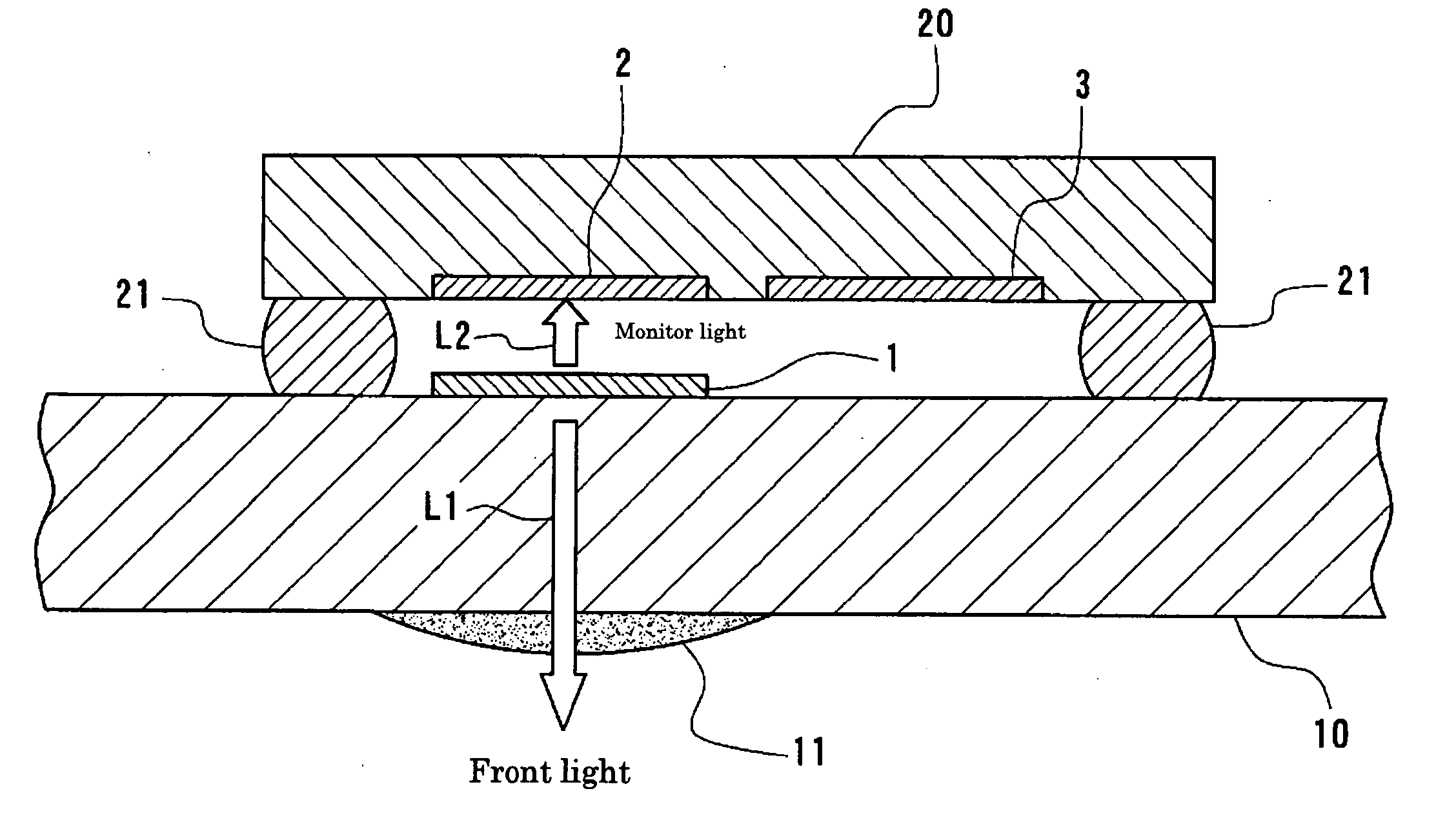
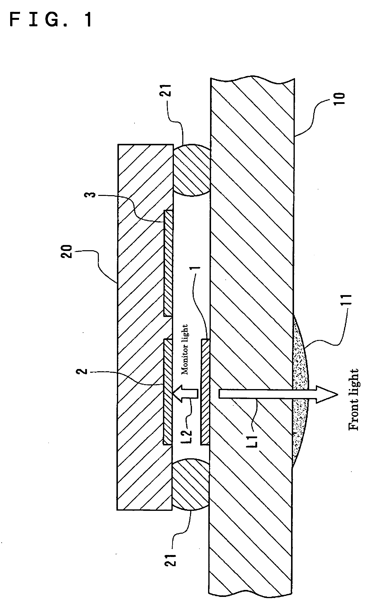
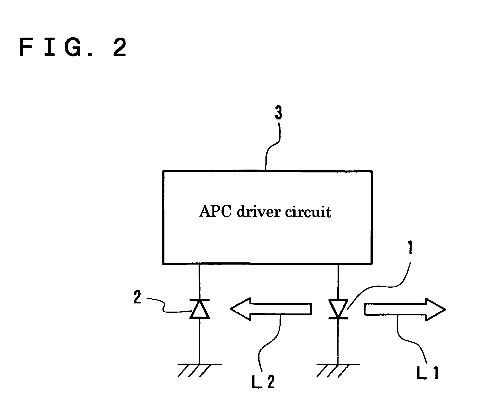
[0072] FIG. 1 is a sectional view schematically showing a semiconductor integrated circuit according to an exemplary embodiment of the invention. The semiconductor integrated circuit includes a transparent substrate 10, a surface-emitting laser 1, and an integrated circuit chip 20. The surface-emitting laser 1 is composed of a micro tile-like element that is adhered to the upper surface of the transparent substrate 10. The integrated circuit chip 20 is flip-chip mounted on the transparent substrate 10.

[0073] The micro tile-like element in which the surface-emitting laser 1 is formed is a micro tile-like (plate) semiconductor device. It is a square plate member. Its depth is several dozen micrometers or less. Its area is several hundred square micrometers or less. The micro tile-like element includes a laser po...


PUM


Abstract

A semiconductor integrated circuit is provided having a surface-emitting laser that makes it possible to precisely monitor the amount of light emitted by the surface-emitting laser for a long period of time, to be miniaturized, and to be easily manufactured. A method to manufacture a semiconductor integrated circuit and electronic equipment is also provided. The semiconductor integrated circuit having a surface-emitting laser includes a transparent substrate, the surface-emitting laser composed of a micro tile-like element that is adhered to the transparent substrate, an integrated circuit chip that is flip-chip mounted on the transparent substrate and is arranged so as to cover the surface-emitting laser and a photodiode that is included in the integrated circuit chip and is arranged so as to face the surface-emitting laser.

Description

[0001] 1. Field of Invention[0002] The present invention relates to a semiconductor integrated circuit having a surface-emitting laser, a manufacturing method of the same, and electronic equipment.[0003] 2. Description of Related Art[0004] Since the efficiency of a semiconductor laser varies depending on ambient temperatures and other factors, it is necessary to monitor and control the amount of laser light from an optical point of view. Some related art edge emitting lasers are mounted on a side of a pillar base called a stem. For such lasers, the amount of laser light is monitored by utilizing rear light.[0005] Unlike edge emitting lasers, it is difficult to utilize rear light for surface-emitting lasers because light is emitted from a semiconductor surface. Therefore, methods to monitor the amount of light shown in FIG. 16 have been invented. As this figure shows, the amount of laser light L10 emitted from a surface-emitting laser 51 is monitored by using reflected light L20 that...

Claims


Application Information

Patent Timeline
Patent Type & Authority Applications(United States)
IPC IPC(8): H01L27/14H01L31/147H01S3/04H01S5/00H01S5/02H01S5/026H01S5/0683H01S5/183
CPCH01L31/147H01S5/02272H01S5/18388H01S5/0683H01S5/02296H01L2224/16225H01L2224/24H01L2224/48465H01L2924/16152H01L2924/19107H01L2924/00014H01S5/02257H01S5/0237H01L2224/0401
Inventor KONDO, TAKAYUKI
Owner SEIKO EPSON CORP
Why Eureka
Try Eureka