Organic light emitting device

a light-emitting device and organic technology, applied in the direction of thermoelectric devices, organic semiconductor devices, other domestic articles, etc., can solve the problem of a large portion of light remaining trapped in the organic layer or the glass substrate, and achieve the effect of improving the light-emitting coupling efficiency

Active Publication Date: 2013-02-14
BEIJING XIAOMI MOBILE SOFTWARE CO LTD
View PDF8 Cites 6 Cited by
  • Summary
  • Abstract
  • Description
  • Claims
  • Application Information

AI Technical Summary

Benefits of technology

[0005]It is an object of the present invention to overcome this prob...

Problems solved by technology

However, a problem with existing devices is that still, a relatively large portion of light remains ...

Method used


Image

  • Organic light emitting device
  • Organic light emitting device

Examples


Embodiment Construction

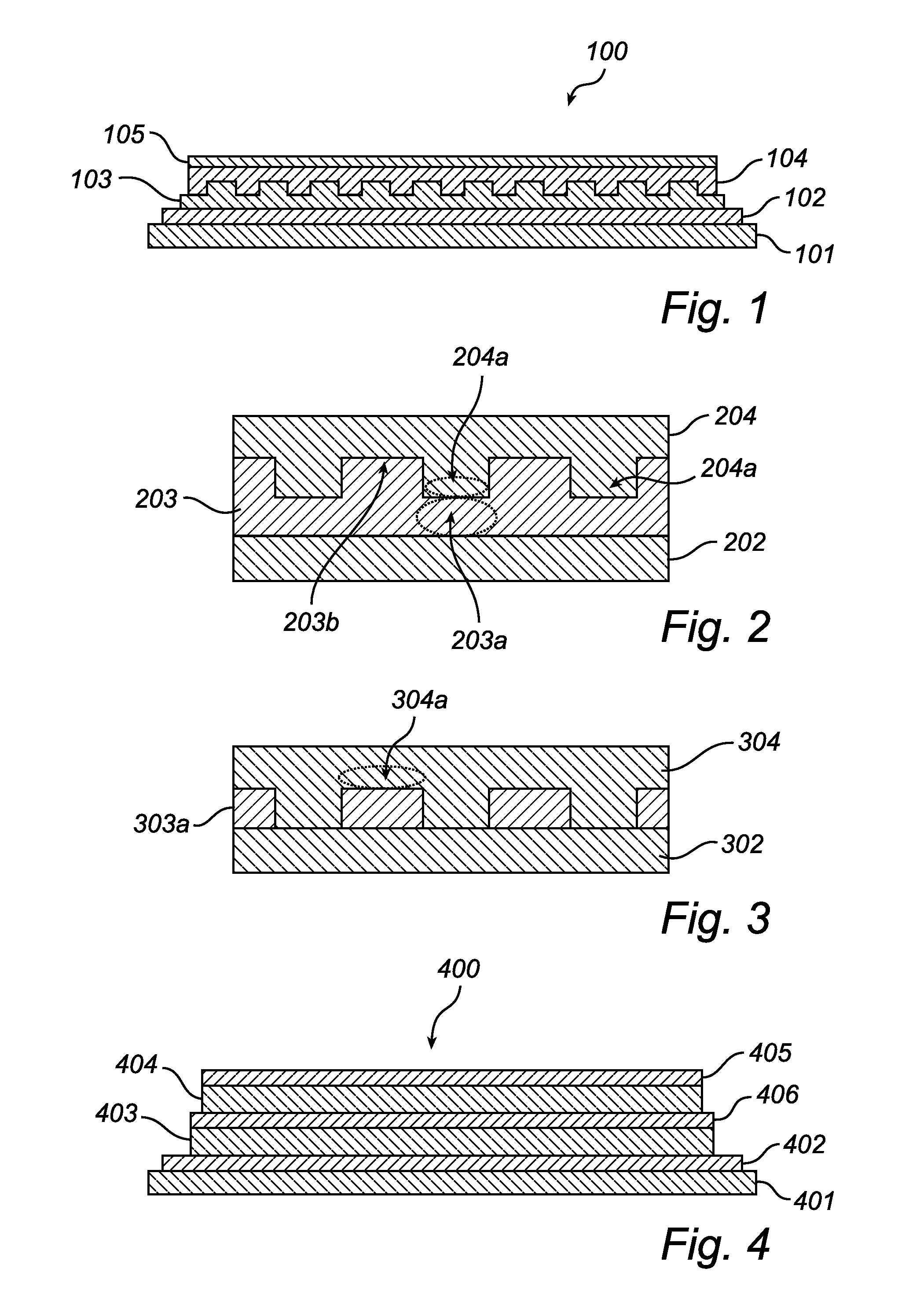
[0039]The present inventors have found that the light out coupling efficiency of an OLED can be improved by providing a layer adjacent the emissive layer, typically a layer located between the emissive layer and the anode, such as a hole transport layer, with an embossed periodic surface structure or by patterning said layer. It has also been found that, alternatively or additionally to the charge transport layer being patterned or provided with said periodic surface structure, the light out coupling efficiency of an OLED can be improved by incorporating an alignment layer between said charge transport layer and said emissive layer, which alignment layer promotes alignment of the optical dipoles of molecules of said light emissive layer towards a common preferred direction.

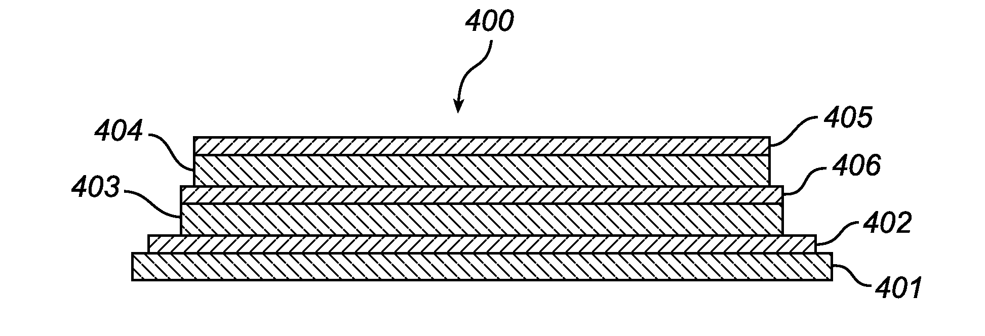
[0040]FIG. 1 illustrates in cross-section an organic light-emitting device according to the present invention. The OLED 100 is arranged on a conventional substrate 101 for bottom-emissive configuration, e.g. a gla...


PUM


Abstract

The invention relates to an organic light-emitting device (OLED) comprising at least: a first electrode (102); a second electrode (105); an organic light emissive layer (104) arranged between said first electrode and said second electrode; and an organic charge transport layer (103) arranged between said first electrode and said emissive layer, wherein i) the charge transport layer is patterned or provided with a periodic surface structure on a surface of the charge transport layer facing the emissive layer, and/or ii) an alignment layer (406) which allows for charge transport to the emissive layer is provided between said charge transport layer and said emissive layer, which alignment layer promotes alignment of the optical dipoles of molecules of said light emissive layer towards a common preferred direction of the molecular axes. The use of the patterned or structured charge transport layer and/or the alignment layer provides improved light out coupling from the OLED layer stack, i.e. increased external quantum efficiency.

Description

FIELD OF THE INVENTION[0001]The present invention relates to an organic light-emitting device (OLED) that is adapted to provide increased light out coupling, and to a method for producing such a device.BACKGROUND OF THE INVENTION[0002]Light emitting diode (LED) based light-emitting devices are today increasingly used for a wide variety of lighting applications. In particular, organic light-emitting devices (OLEDs) are increasingly used for signage lighting, such as advertising information and indication signs.[0003]For commercialization of OLEDs, device efficiency is an important parameter. The total device efficiency is determined by the internal quantum efficiency and the external quantum efficiency (light out coupling). In recent years many techniques have been proposed to improve the internal quantum efficiency, including for example doping of transport layers to increase charge recombination, and the use of triplet-emitter by which almost 100% internal quantum efficiency can be...

Claims


Application Information

Patent Timeline
IPC IPC(8): H01L51/50H01L51/40
CPCH01L51/5048H01L51/5265H01L51/5293H01L2251/105H01L2251/558H01L51/5275H10K50/14H10K50/15H10K50/852H10K50/868H10K50/858H10K71/821H10K2102/351Y10S428/917H10K71/211H10K71/00
Inventor STROMER, JAN FRANKVERSCHUUREN, MARKUS ANTONIUSDE LEEUW, DAGOBERT MICHELBERNARDS, THOMAS NICOLAAS MARIA
Owner BEIJING XIAOMI MOBILE SOFTWARE CO LTD
Why Eureka
Try Eureka