Light emitting device and method for manufacturing light emitting device

a technology of light emitting devices and light emitting devices, which is applied in the direction of semiconductor devices, electrical devices, basic electric elements, etc., can solve the problems of reducing light extraction efficiency, long-term reliability concerns, and loss of light due to absorption loss, so as to improve light extraction efficiency, prevent light leakage from the bottom surface of the base member, and achieve the effect of high outpu

Active Publication Date: 2013-02-14
NICHIA CORP
View PDF5 Cites 87 Cited by
  • Summary
  • Abstract
  • Description
  • Claims
  • Application Information

AI Technical Summary

Benefits of technology

[0067]With the light emitting device according to the present invention, absorption of light due to the conductive portions such as the electrically conductive member can be suppressed, so that light from the light emitting element can be extracted efficiently, which allows obtaining higher output. Further, according to the light emitting device according to the present invention, leakage of light from the bottom surface of the base member can be prevented by coating the slit in the conductive portion with the filler, so that light from the light emitting element can be extracted more efficiently and thus higher optical output power can be achieved.
[0068]In the light emitting device described above, insulating filler capable of reflecting light is applied so that the light extracting efficiency can be improved without using a specific material which has a high reflectance for the electrically conductive member. Further, the insulating filler is formed with a greater thickness, so that discoloration and corrosion of the electrically conductive member can be suppressed. With such an arrangement as described above, reliability can be improved.
[0069]Further, with the light emitting device according to the present invention, the reflectice member is formed around the electrodes of the light emitting element, so that a structure which allows little leakage of light in the downward direction can be obtained. Thus, optical loss due to the light entering under the light emitting element can be reduced. Also, the reflective member reflects light which enters under the light emitting element, so that the light extracting efficiency can be improved.
[0070]According to a method of manufacturing a light emitting device according to the present invention, a light emitting device of high optical output and high reliability can be manufactured. According to a method of manufacturing a light emitting device according to the present invention, a reflective member is formed around the electrodes of the light emitting elements so that optical loss due to light propagates downward of the light emitting elements can be reduced. Also, the reflective member reflects light which enters under the light emitting element, so that the light extracting efficiency can be improved.

Problems solved by technology

However, loss due to absorption of light (absorption loss of light) occurs depending on the materials of the base member, electrically conductive members, sealing member, etc.
Particularly, the surface area of the electrically conductive members is relatively large, absorption loss of light by the electrically conductive members may reduce light extraction efficiency.
Disposing of a member having high reflectance in the light emitting device is viewed as a way to suppress optical absorption by the members used in the light emitting device, but among those materials having high reflectance (such as silver), some materials are subjected to sulfuration or halogenation and may cause longterm reliability concerns.
That is, there has been a problem in which, discoloration due to sulfuration or halogenation of the material by the sulfur component etc., contained in the atmosphere causes reduction of the reflectance of the material, which results in reduction of the light extracting efficiency.

Method used


Image

  • Light emitting device and method for manufacturing light emitting device
  • Light emitting device and method for manufacturing light emitting device
  • Light emitting device and method for manufacturing light emitting device

Examples


first embodiment

[0105]In a first embodiment, a light emitting device which uses a FD element will be described. First, a general construction of a light emitting device will be described with description of each component, then, the material or the like of each member will be described.

[0106]

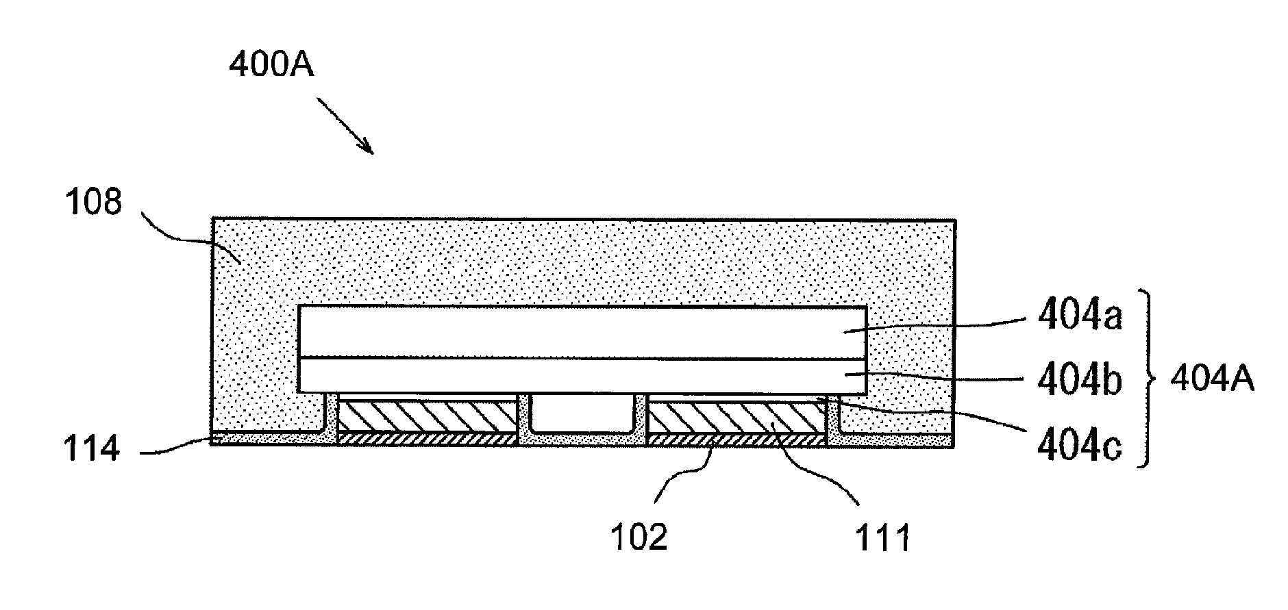
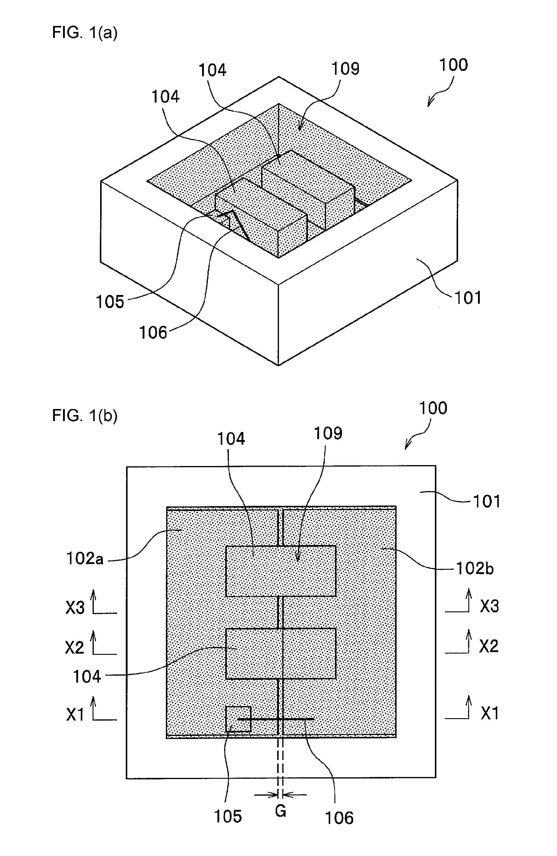
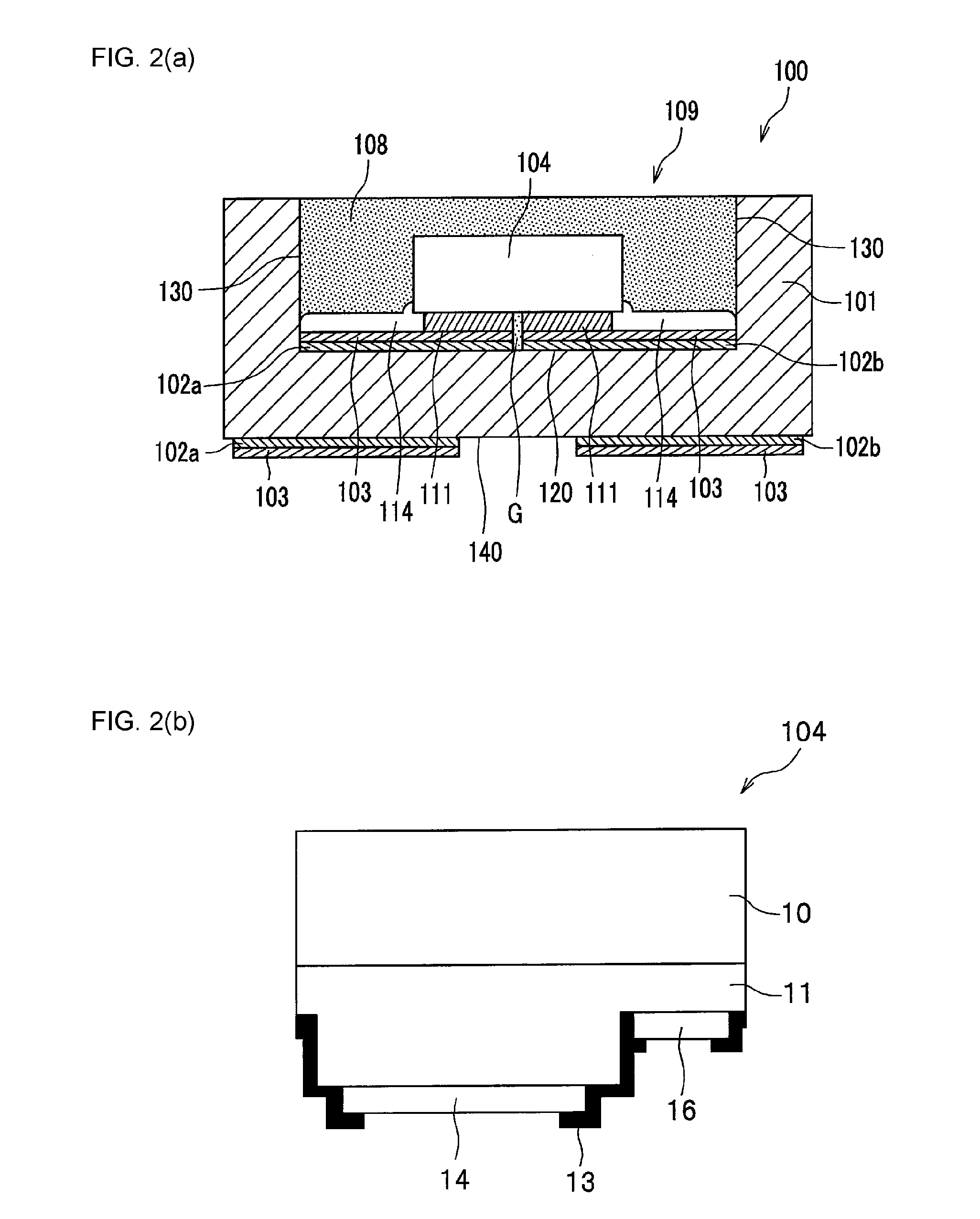
[0107]As shown in FIG. 1 and FIG. 2, the light emitting device 100 includes a light emitting element 104 having a semiconductor layer 11 and a transparent substrate (hereinafter may be referred to as a substrate) 10, a reflective member 114 applied so that at least a portion of a side surface and the upper surface of the transparent substrate 10 are exposed and a side surface of the semiconductor layer 11 is covered therewith, and the light transmissive member 108 which covers the portions exposed from the reflective member 114.

[0108]In the present embodiment, as shown in FIG. 1 and FIG. 2, the light emitting device 100 is a light emitting device 100 having at least one light emitting element 104 (two are shown...

second embodiment

[0203]A light emitting device which uses a FU element will be described in a second embodiment. FIG. 13 shows a perspective view of an example of a light emitting device according to the present embodiment. First, a general construction of a light emitting device will be described with description of each component, then, the material or the like of each member will be described. In what follows, the different points from the above embodiment of the light emitting device 100 will be mainly described.

[0204](General Construction)

[0205]As shown in FIG. 7 and FIG. 8, a light emitting device 200 is a device in which at least one light emitting element 204 (two in the figures) are mounted, and mainly includes a base member 201, electrically conductive members 202a, 202b, 202c disposed on the base member 201, light emitting element 204 mounted on the respective portions of the electrically conductive members 202a, 202b, 202c, a wire 206 which connects a portion of the electrically conducti...

third embodiment

[0244]A light emitting device which uses a FD element will be described in a third embodiment. First, a general construction of a light emitting device will be described with description of each component, then, the material or the like of each member will be described. In what follows, the different points from the above embodiment of the light emitting device 100 will be mainly described.

[0245]

[0246]As shown in FIG. 14 and FIG. 15, the light emitting device 100 includes a light emitting element 104 having a semiconductor layer 11 and a transparent substrate 10, a reflective member 114 applied so that at least a portion of a side surface and the upper surface of the transparent substrate 10 are exposed and a side surface of the semiconductor layer 11 is covered therewith, and the light transmissive member 108 which covers the portions of the transparent substrate 10 exposed from the reflective member 114.

[0247]In the present embodiment, as shown in FIG. 14 and FIG. 15, the light em...


PUM


Abstract

A light emitting device (100) includes a base member (101), electrically conductive members (102a, 102b) disposed on the base member (101), a light emitting element (104) mounted on the electrically conductive members (102a, 102b), an insulating filler (114) covering at least a portion of surfaces of the electrically conductive members (102a, 102b) where the light emitting element (104) is not mounted, and a light transmissive member (108) covering the light emitting element (104).

Description

BACKGROUND OF THE INVENTION[0001]1. Technical Field[0002]The present invention relates to a light emitting device applicable to purposes such as an indicator, a lighting apparatus, a display, a backlight light source for liquid crystal display, and a method of manufacturing the light emitting device.[0003]2. Description of Background Art[0004]In recent years, various semiconductor devices have been proposed and are put in practical use, and the demand for high performance is ever increasing. In particular, electric components are required to have high reliability to maintain performance for a long period of time, in other words, to maintain stable operation for a long period of time, even under severe environment. The same applies for light emitting diodes (LEDs) and other light emitting devices. Requirements for higher performance in the area of general lighting, in-vehicle lighting, and the like, is growing daily, and further higher output (higher luminance) and higher reliability...

Claims


Application Information

Patent Timeline
Patent Type & Authority Applications(United States)
IPC IPC(8): H01L33/60
CPCH01L33/60H01L2933/005H01L25/167H01L33/486H01L33/54H01L2224/48137H01L2224/48227H01L2224/73265H01L2224/45144H01L2224/83192H01L2224/92247H01L25/0753H01L2224/49175H01L2224/8592H01L2924/01322H01L2924/00H01L24/48H01L2224/48139H01L2224/48228H01L2224/73204H01L2924/014H01L2924/09701H01L2924/12041H01L2924/3025H01L2224/45015H01L2224/45124H01L2224/45147H01L2224/45169H01L2924/00014H01L2924/12035H01L2924/12042H01L2924/12044H01L24/45H01L2924/181H01L24/49H01L33/56H01L2924/2076H01L2224/05599H01L2924/00012H01L33/44H01L33/50H01L33/62H01L33/52H01L2924/01004H01L2924/01012H01L2924/01013H01L2924/01025H01L2924/01029H01L2924/0103H01L2924/01032H01L2924/01033H01L2924/01038H01L2924/01047H01L2924/0105H01L2924/01058H01L2924/01079H01L2924/01082H01L2924/01005H01L2924/01006H01L2924/01024H01L2924/01042H01L2924/01045H01L2924/01063H01L2924/01065H01L2924/01074H01L2924/01077H01L2924/01078H01L2924/01014H01L2924/01028H01L33/005H01L33/483
Inventor YAMADA, MOTOKAZUSENO, RYOTAKAMADA, KAZUHIRO
Owner NICHIA CORP
Why Eureka
Try Eureka