
Eureka
For R&D, Eureka makes reading and utilizing patents & technical documents easy.
Eureka AIR
Designed for self-driven R&D workflows. Generate viable solutions, solve complex R&D challenges, empower your innovation with AI.

Eureka Materials
Designed for material experts only. Revolutionize your material R&D, from search, analyze, to developing new materials.

TechResearch
Generate reliable direction feasibility study reports for your R&D in just a few steps.

TechSeek
Discover and master advanced knowledge NOW. Basics, ideas, possibilities, all at once.

TechMind
As an expert in R&D Theories, TechMind can generates customized viable solutions instantly.

TechRisk
Analyze your overall solution with one click, know your potential R&D risks in advance.

TechMonitor
Get weekly tech updates, stay abreast of the latest tech innovations and key insights.
Semiconductor device reducing risks of a wire short-circuit and a wire flow
- Summary
- Abstract
- Description
- Claims
- Application Information
AI Technical Summary
Benefits of technology
Problems solved by technology
Method used
Image

Examples
first exemplary embodiment
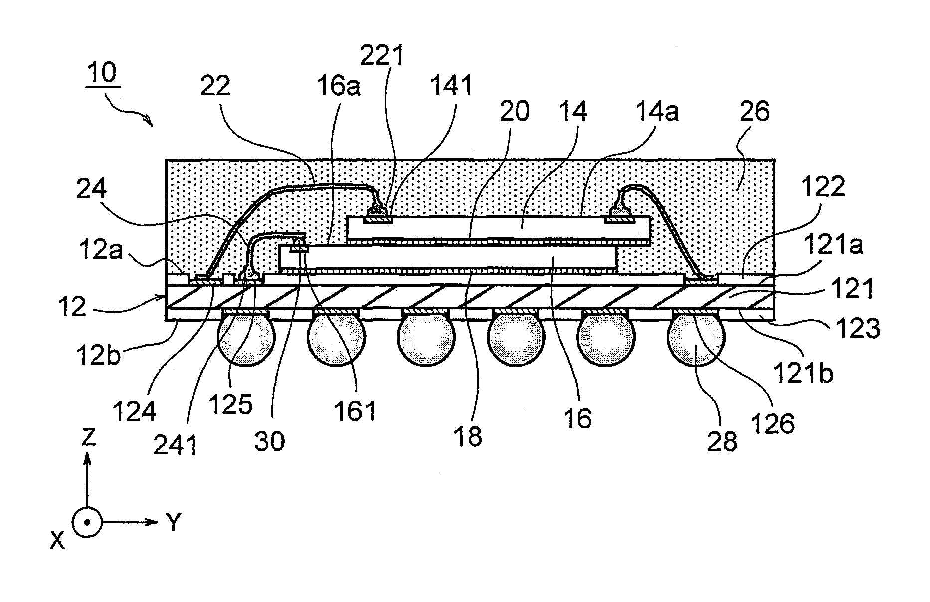
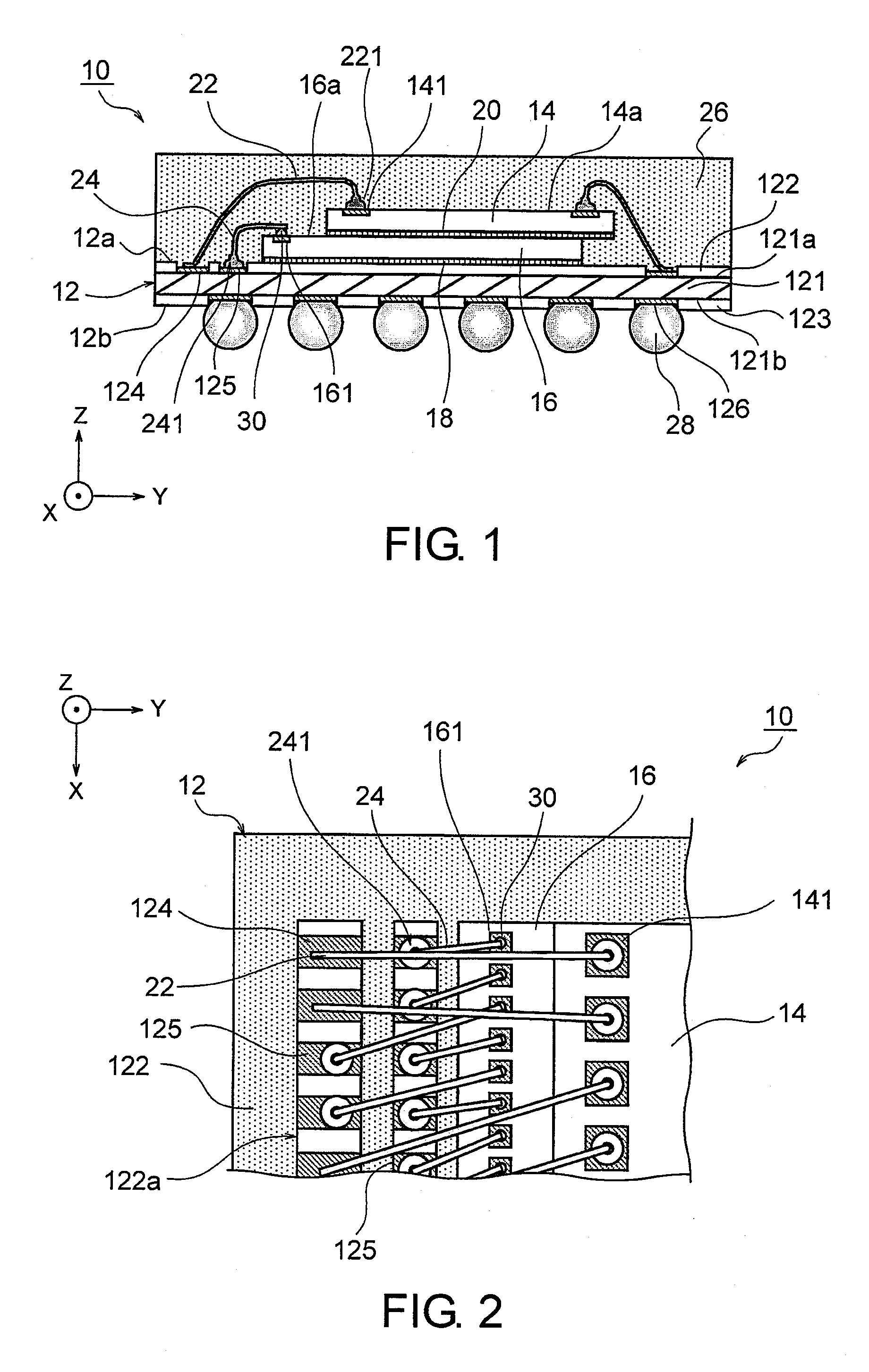
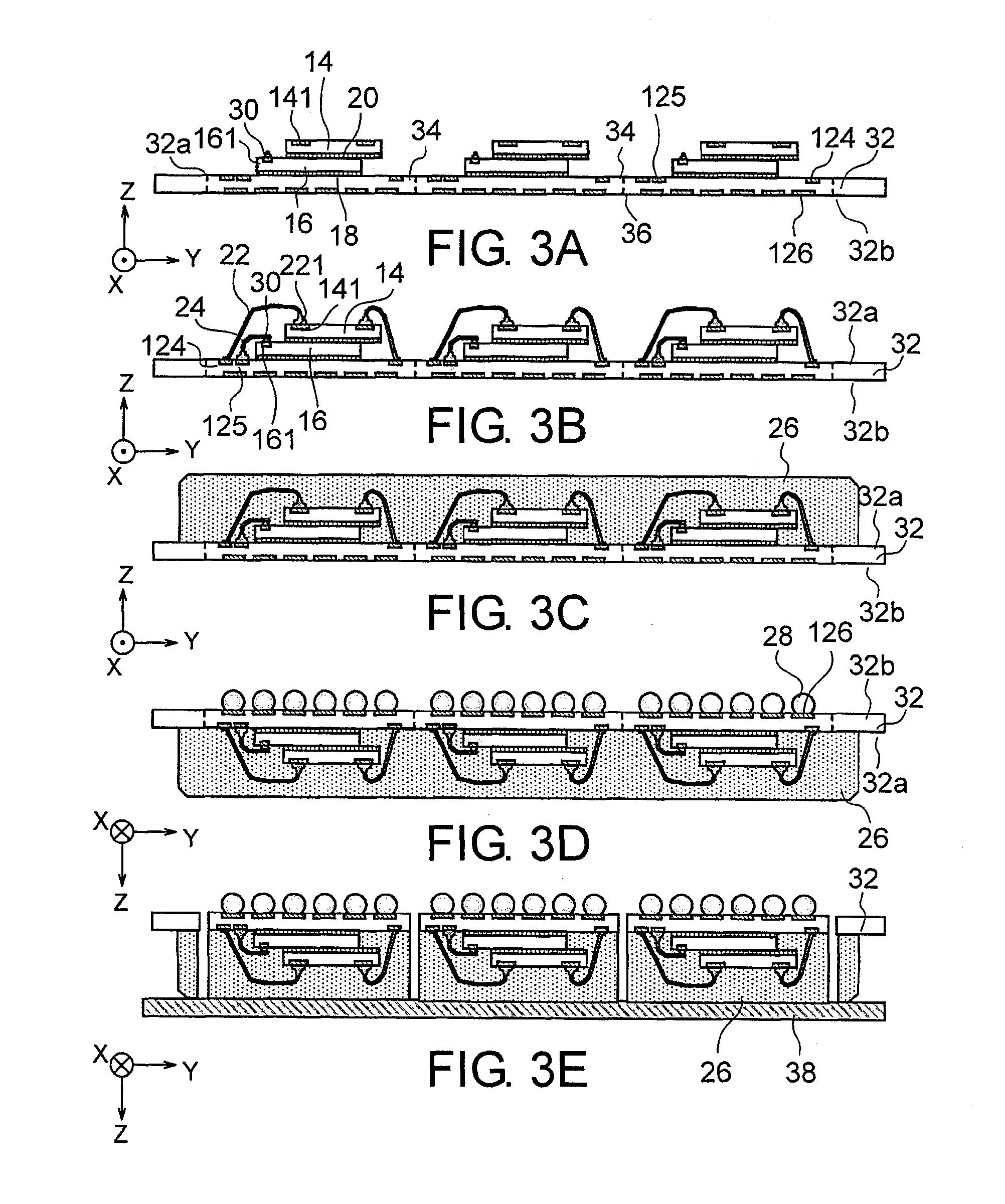
[0034]Referring now to FIGS. 1 and 2, the description will proceed to an MCP type semiconductor device 10 according to a first exemplary embodiment of this invention. FIG. 1 is a cross-sectional view schematically showing the MCP type semiconductor device 10 and FIG. 2 is a plan view showing a main part of a wire connection portion of the MCP type semiconductor device 10. In the plan view of FIG. 2, a sealing resin (denoted by the reference numeral 26 in FIG. 1) is omitted from the illustration.
[0035]Herein, in the manner shown in FIGS. 1 and 2, an orthogonal coordinate system (X, Y, Z) is used. In a state illustrated in FIGS. 1 and 2, in the orthogonal coordinate system (X, Y, Z), an X-axis direction is a fore-and-aft direction (a depth direction), a Y-axis direction is a left-and-right direction (a width direction), and a Z-axis direction is an up-and-down direction (a height direction).
[0036]The illustrated semiconductor device 10 comprises a wiring substrate 12, a first semicond...
first modified example
[0073]Referring to FIG. 4, the description will proceed to an MCP type semiconductor device 10A according to a first modified example of the first exemplary embodiment of this invention. FIG. 4 is a cross-sectional view showing a main portion of the MCP type semiconductor device 10A. In the first modified example, the same elements as in the MCP type semiconductor device 10 illustrated in FIGS. 1 and 2 are denoted by the same reference numerals, and the description will be made as regards only differences for the sake of simplification of the description.
[0074]The illustrated semiconductor device 10A is similar in structure to the semiconductor device 10 according to the first exemplary embodiment except that a spacer 40 comprising a silicon substrate and a third adhesive member 42 are inserted between the first semiconductor chip 14 and the second semiconductor chip 16. In addition, the first semiconductor chip 14 and the second semiconductor chip 16 are stacked to each other witho...
second modified example
[0077]Referring to FIG. 5, the description will proceed to an MCP type semiconductor device 10B according to a second modified example of the first exemplary embodiment of this invention. FIG. 5 is a cross-sectional view showing a main portion of the MCP type semiconductor device 10B. In the second modified example, the same elements as in the MCP type semiconductor device 10 illustrated in FIGS. 1 and 2 are denoted by the same reference numerals, and the description will be made as regards only differences for the sake of simplification of the description.
[0078]The illustrated semiconductor device 10B is similar in structure to the semiconductor device 10 according to the first exemplary embodiment except that an adhesive member 44 enable to embed and bond wires are inserted between the first semiconductor chip 14 and the second semiconductor chip 16. As such an adhesive member 44, for example, a film on wire (FOW) may be used. In addition, the first semiconductor chip 14 and the s...
PUM
 Abstract
Description
Claims
Application Information
 - R&D Engineer
- R&D Manager
- IP Professional
- Industry Leading Data Capabilities
- Powerful AI technology
- Patent DNA Extraction
Browse by: Latest US Patents, China's latest patents, Technical Efficacy Thesaurus, Application Domain, Technology Topic, Popular Technical Reports.
© 2024 PatSnap. All rights reserved.Legal|Privacy policy|Modern Slavery Act Transparency Statement|Sitemap|About US| Contact US: help@patsnap.com