
Power overlay structure with leadframe connections

a power overlay and leadframe technology, applied in semiconductor devices, semiconductor/solid-state device details, electrical apparatus, etc., can solve problems such as failures of solder joints and easy early failure of connections, and achieve high reliability

Active Publication Date: 2013-02-21
GENERAL ELECTRIC CO
View PDF6 Cites 11 Cited by
  • Summary
  • Abstract
  • Description
  • Claims
  • Application Information

AI Technical Summary

Benefits of technology

The invention provides a semiconductor device package structure that eliminates the use of solder ball grid arrays (BGAs) or land grid arrays (LGAs) to connect the POL package to an external circuit. Instead, a leadframe connection is provided for the POL package to provide a highly reliable interconnection structure usable in a variety of high stress environments. The method also includes providing a leadframe for the POL sub-module that is configured to make an interconnection between the POL sub-module and an external circuit structure, and encapsulating the POL sub-module and a portion of the leadframe with a polymeric material to provide structural rigidity to the POL structure. This allows for a more reliable and durable connection between the semiconductor device and external circuit.

Problems solved by technology

While the short stand-off height (˜5 to 20 mils) of these types of interconnections provides a low profile, such connections are susceptible to early failure in high stress conditions.
That is, very large temperature cycling ranges, shock, and vibration can induce failures in these solder joints.

Method used


Image

  • Power overlay structure with leadframe connections
  • Power overlay structure with leadframe connections
  • Power overlay structure with leadframe connections

Examples


Embodiment Construction

[0016]Embodiments of the present invention provide for a semiconductor device package having leadframe connections incorporated therein, as well as a method of forming such a semiconductor device package. The semiconductor device package is manufactured such that the leadframe connections form a highly reliable interconnection structure, usable in a variety of high stress environments, for attaching the semiconductor device package to an external circuit.

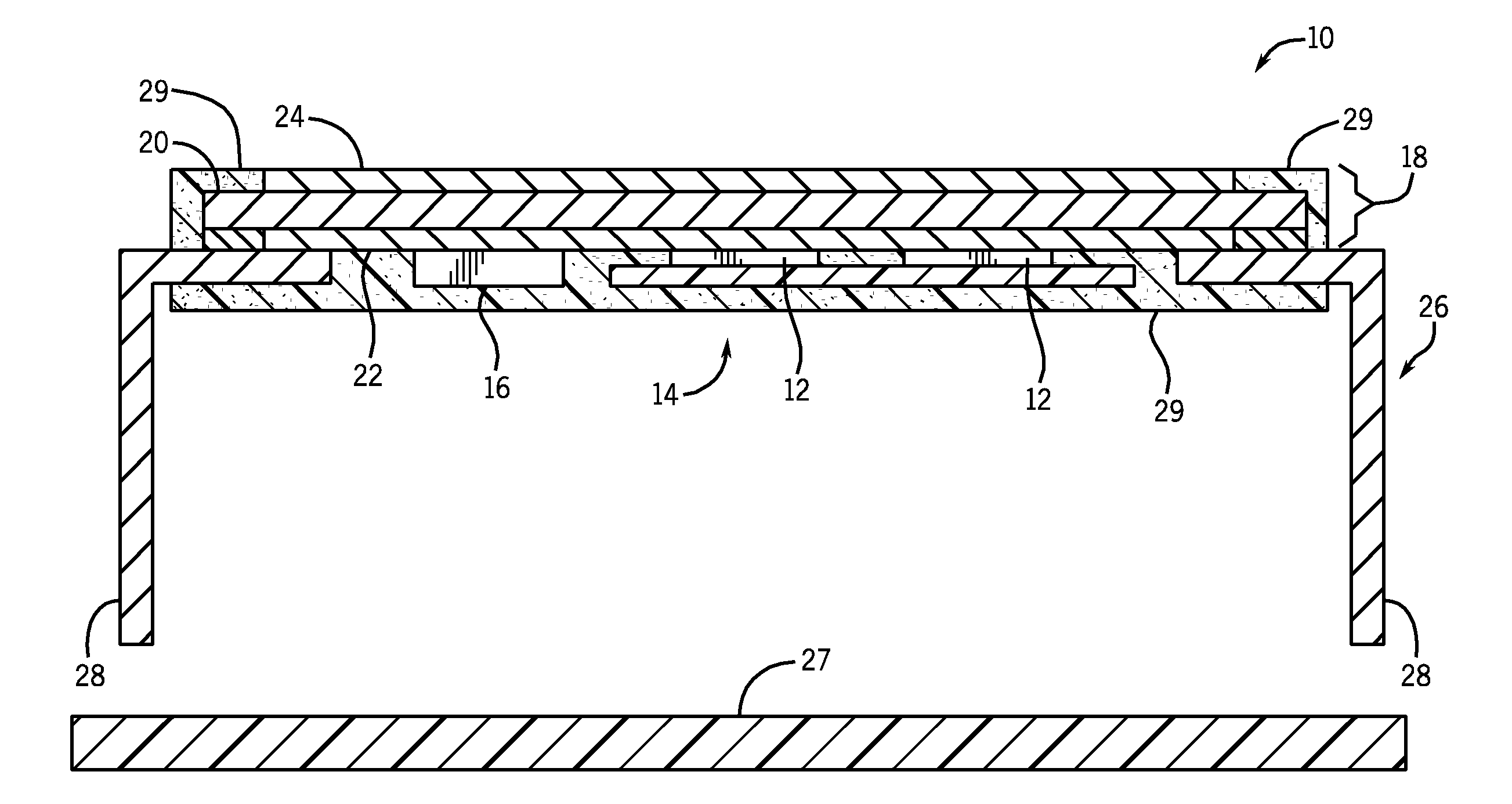
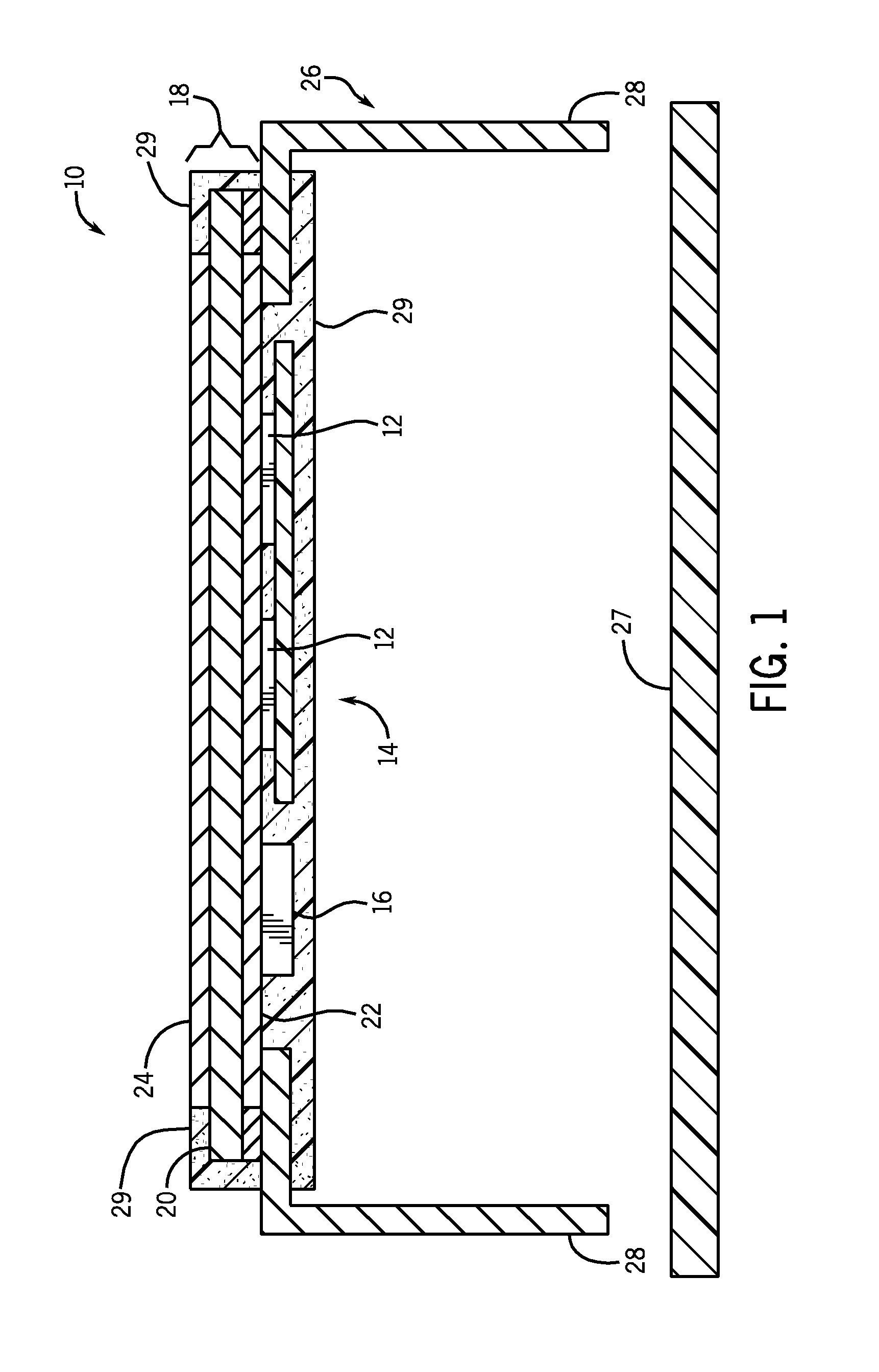
[0017]Referring to FIG. 1, a power overlay (POL) packaging and interconnect structure 10 is shown according to an embodiment of the invention. The POL structure 10 includes one or more semiconductor device(s) 12 therein that, according to various embodiments, may be in the form of a die, diode, or other power electronic device. As shown in FIG. 1, two semiconductor device(s) 12 are provided in POL structure 10, however, it is recognized that a greater or lesser number of semiconductor devices 12 could be included in POL structure 10...


PUM


Abstract

A power overlay (POL) packaging structure that incorporates a leadframe connection is disclosed. The a POL structure includes a POL sub-module having a dielectric layer, at least one semiconductor device attached to the dielectric layer and that includes a substrate composed of a semiconductor material and a plurality of connection pads formed on the substrate, and a metal interconnect structure electrically coupled to the plurality of connection pads of the at least one semiconductor device, with the metal interconnect structure extending through vias formed through the dielectric layer so as to be connected to the plurality of connection pads. The POL structure also includes a leadframe electrically coupled to the POL sub-module, with the leadframe comprising leads configured to make an interconnection to an external circuit structure.

Description

BACKGROUND OF THE INVENTION[0001]Embodiments of the invention relate generally to structures and methods for packaging semiconductor devices and, more particularly, to a power overlay (POL) packaging structure that incorporates a leadframe connection therein.[0002]Power semiconductor devices are semiconductor devices used as switches or rectifiers in power electronic circuits, such as switched mode power supplies, for example. Most power semiconductor devices are only used in commutation mode (i.e., they are either on or off), and are therefore optimized for this. Many power semiconductor devices are used in high voltage power applications and are designed to carry a large amount of current and support a large voltage. In use, high voltage power semiconductor devices are connected to an external circuit by way of a power overlay (POL) packaging and interconnect system, with the POL package also providing a way to remove the heat generated by the device and protect the device from th...

Claims


Application Information

Patent Timeline
Patent Type & Authority Applications(United States)
IPC IPC(8): H01L23/495H01L21/50
CPCH01L23/3735H01L23/49531H01L23/49575H01L23/49811H01L24/24H01L24/29H01L24/82H01L24/83H01L25/072H01L2224/24137H01L2224/24226H01L2224/24246H01L2224/29339H01L2224/32225H01L2224/32245H01L2224/48H01L2224/73217H01L2224/73267H01L2224/83192H01L2224/83424H01L2224/83447H01L2224/83801H01L2224/8384H01L2224/8385H01L2224/83855H01L2224/92144H01L2924/1203H01L2924/16152H01L2924/19105H01L2224/29101H01L2924/01029H01L21/50H01L23/495H01L2924/014H01L2924/00014H01L2924/19041H01L2924/19042H01L2924/19043H01L2924/00015H01L2924/00H01L2924/15747H01L25/50H01L2224/04105H01L2924/12042H01L2924/181H01L2924/00012
Inventor GOWDA, ARUN VIRUPAKSHAMCCONNELEE, PAUL ALAN
Owner GENERAL ELECTRIC CO
Learn More