Semiconductor devices and methods of manufacturing the same

a technology of semiconductors and semiconductors, applied in the direction of semiconductor devices, electrical equipment, transistors, etc., can solve the problems of reducing the operation speed of transistors, and achieve the effect of improving reliability and manufacturing methods

Active Publication Date: 2013-02-21
SAMSUNG ELECTRONICS CO LTD
View PDF6 Cites 26 Cited by
  • Summary
  • Abstract
  • Description
  • Claims
  • Application Information

AI Technical Summary

Benefits of technology

[0009]Exemplary embodiments of the inventive concept provide semiconductor devices with improved reliability and methods of manufacturing the same.
[0011]Exemplary embodiments of the inventive concept provide semiconductor devices which can increase a turn-on current of a transistor, and methods of manufacturing the same.

Problems solved by technology

However, the decrease in the turn-on current of the transistor may cause a decrease in the operation speed of the transistor.

Method used


Image

  • Semiconductor devices and methods of manufacturing the same
  • Semiconductor devices and methods of manufacturing the same
  • Semiconductor devices and methods of manufacturing the same

Examples


Embodiment Construction

[0059]Hereinafter, exemplary embodiments of the inventive concept will be described in detail with reference to the accompanying drawings. The inventive concept may, however, be embodied in many different forms and should not be construed as limited to the exemplary embodiments set forth herein. Certain aspects of the drawings may be exaggerated for clarity.

[0060]It will be understood that when an element such as a layer, region or substrate is referred to as being “connected” or “coupled” to another element, it may be directly connected or coupled to the other element or intervening elements may be present.

[0061]Similarly, it will be understood that when an element such as a layer, region or substrate is referred to as being “on” another element, it can be directly on the other element or intervening elements may be present.

[0062]Like reference numerals may denote like elements throughout the specification and drawings, unless otherwise noted.

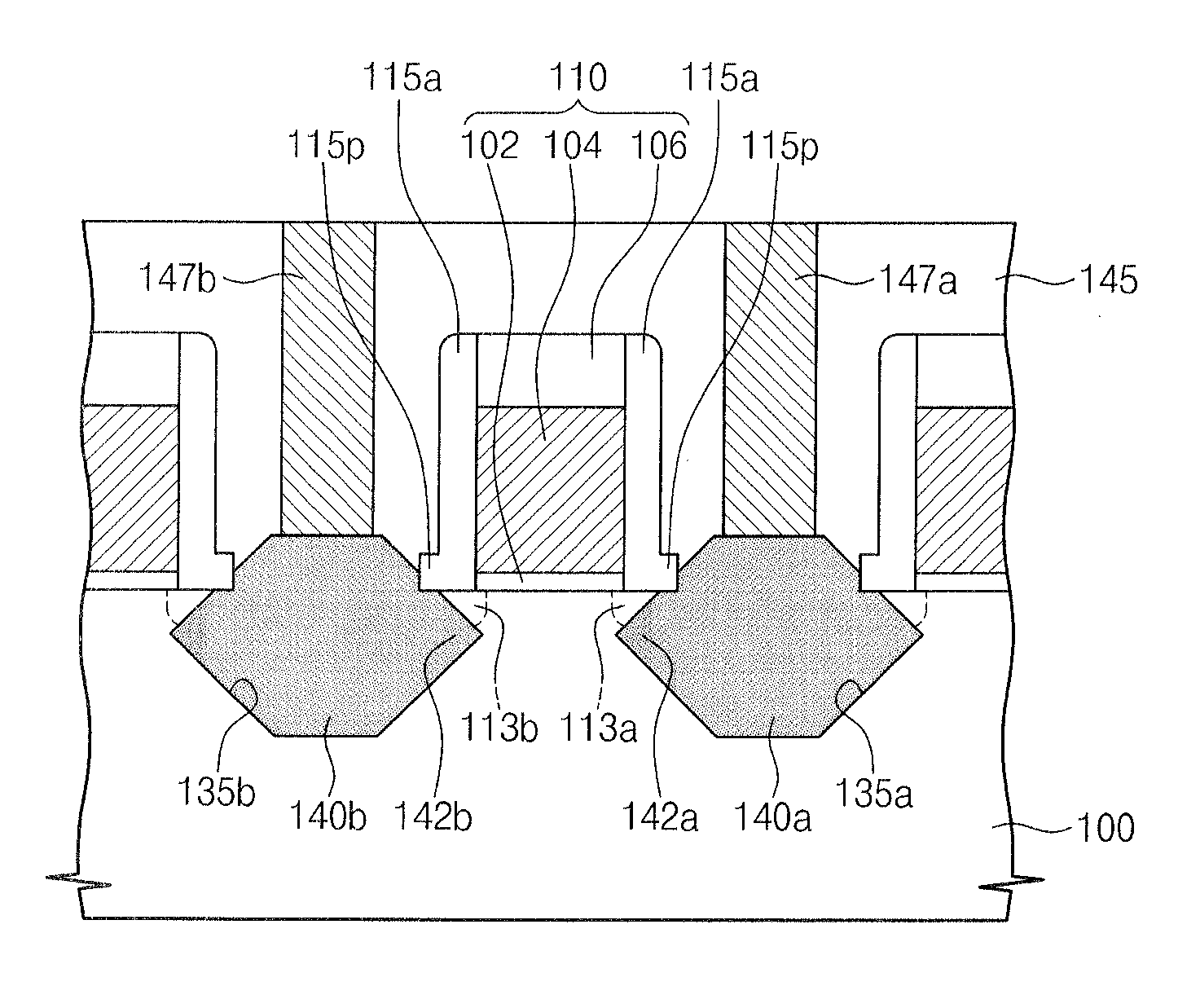
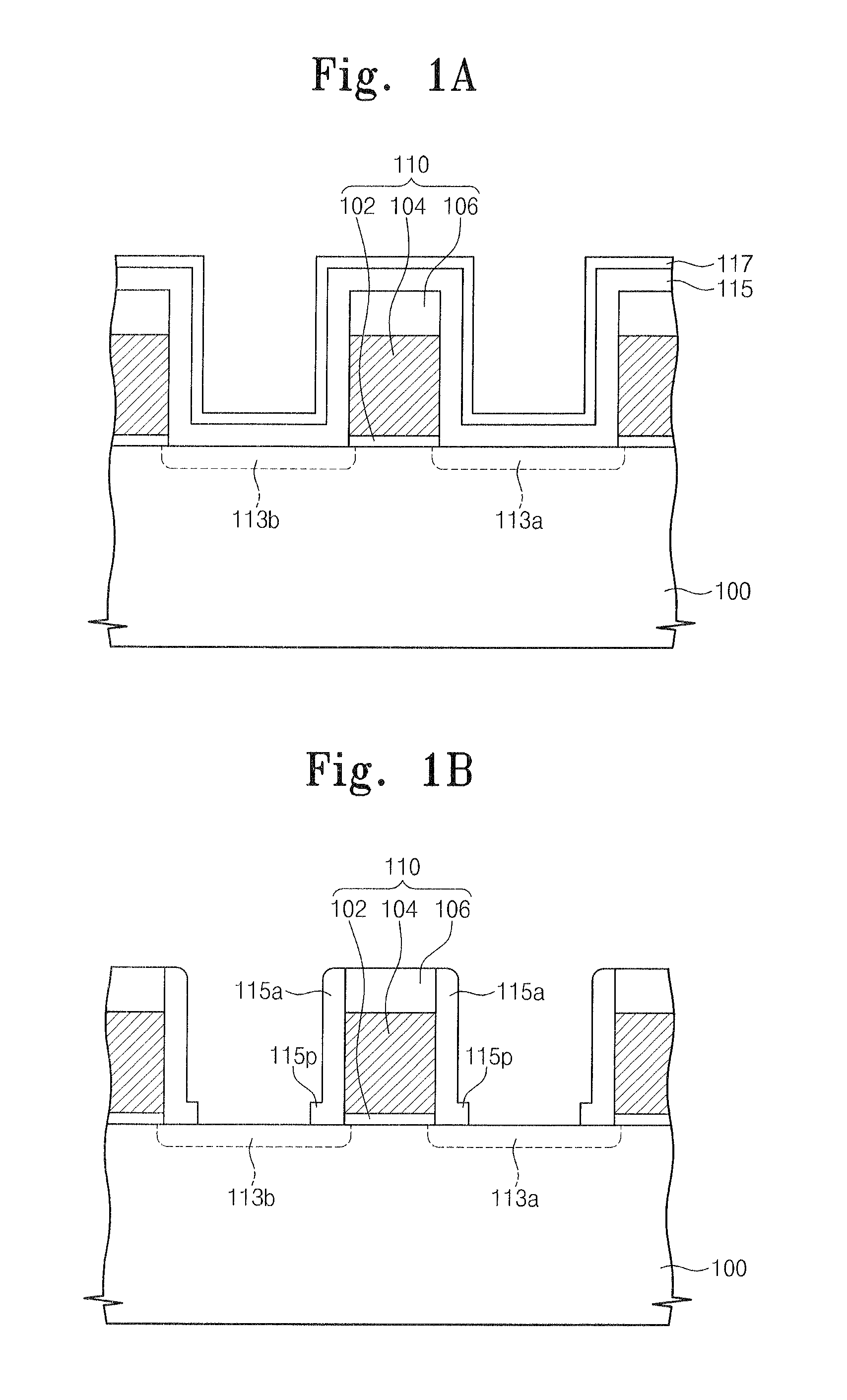
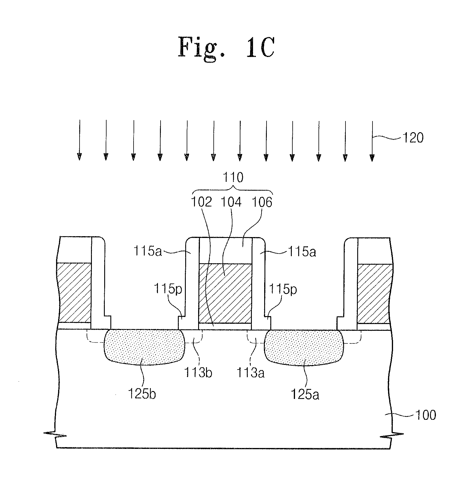
[0063]FIGS. 1A through 1G are cross-sec...


PUM

PropertyMeasurementUnit
temperatureaaaaaaaaaa
angleaaaaaaaaaa

Abstract

A method of manufacturing a transistor of a semiconductor device, the method including forming a gate pattern on a semiconductor substrate, forming a spacer on a sidewall of the gate pattern, wet etching the semiconductor substrate to form a first recess in the semiconductor substrate, wherein the first recess is adjacent to the spacer, and wet etching the first recess to form a second recess in the semiconductor substrate.

Description

CROSS-REFERENCE TO RELATED APPLICATION[0001]This U.S. non-provisional patent application claims priority under 35 U.S.C. §119 to Korean Patent Application No. 10-2011-0082715, filed on Aug. 19, 2011, the disclosure of which is incorporated by reference herein in its entirety.BACKGROUND[0002]1. Technical Field[0003]The present inventive concept relates to semiconductor devices and methods of manufacturing the same.[0004]2. Discussion of the Related Art[0005]Semiconductor devices are used in almost every industrial field, including various electronic devices, vehicles, vessels and so forth. A field effect transistor (hereinafter referred to as a transistor) is a fundamental building block of modern semiconductor devices.[0006]Some transistors are packaged individually, but many more are found embedded in integrated circuits.[0007]The transistor may include a source and a drain spaced apart from each other in a semiconductor substrate, and a gate electrode covering the top surface of a...

Claims


Application Information

Patent Timeline
Patent Type & Authority Applications(United States)
IPC IPC(8): H01L21/20H01L21/425
CPCH01L21/26506H01L21/76237H01L21/26593H01L21/30604H01L21/30608H01L21/324H01L29/6653H01L29/66545H01L29/6659H01L29/66621H01L29/66636H01L29/7834H01L29/7835H01L29/7848H01L29/0847H01L29/1037H01L29/165H01L21/26586H01L29/045
Inventor KIM, SEOKHOONKIM, SANGSUKOH, CHUNG GEUNLEE, BYEONGCHANLEE, SUNGHILJOE, JINYEONG
Owner SAMSUNG ELECTRONICS CO LTD
Why Eureka
Try Eureka