Organic light emitting diode display device for pixel current sensing and pixel current sensing method thereof

a technology of organic light-emitting diodes and display devices, which is applied in the direction of instruments, computing, electric digital data processing, etc., can solve the problems of reduced lifespan of amoled display panels or residual images, increased circuit size, and difficulty in high-speed current sensing

Active Publication Date: 2013-02-28
LG DISPLAY CO LTD
View PDF9 Cites 214 Cited by
  • Summary
  • Abstract
  • Description
  • Claims
  • Application Information

AI Technical Summary

Benefits of technology

[0011]An object of the present invention is to provide an OLED display device which can sense a current of each pixel at high speed by a simple structure in order to compensate for a luminance deviation between pixels and a pixel current sensing method thereof.

Problems solved by technology

Generally, an initially generated characteristic difference of a driving TFT results in spots or patterns on a screen and a characteristic difference caused by degradation of the driving TFT produced while the OLED is driven reduces the lifespan of an AMOLED display panel or generates a residual image.
However, the above patent in which a method for sensing a current flowing to a power line (VDD or VSS) of a panel while lighting up each pixel is used delays a current sensing time due to a parasitic capacitor existing in parallel to the power line when resolution is increased, thereby making it difficult to perform high-speed current sensing.
In addition, although currents of a plurality of pixels can simultaneously sense at high speed using a plurality of current sensing circuits, circuit size is increased and therefore such a method is not practical.
However, it is difficult to sense and compensate for a characteristic deviation due to degradation of the driving TFT generated while the OLED is driven after product shipment.

Method used


Image

  • Organic light emitting diode display device for pixel current sensing and pixel current sensing method thereof
  • Organic light emitting diode display device for pixel current sensing and pixel current sensing method thereof
  • Organic light emitting diode display device for pixel current sensing and pixel current sensing method thereof

Examples


Embodiment Construction

[0071]Reference will now be made in detail to the exemplary embodiments of the present invention, examples of which are illustrated in the accompanying drawings. Wherever possible, the same reference numbers will be used throughout the drawings to refer to the same or like parts.

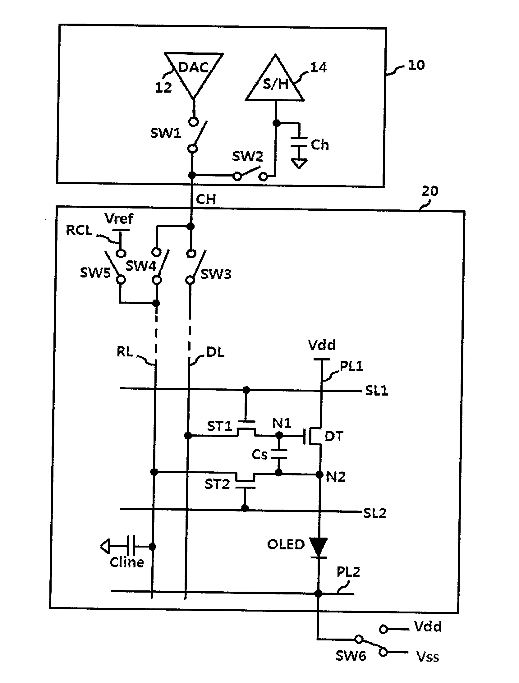
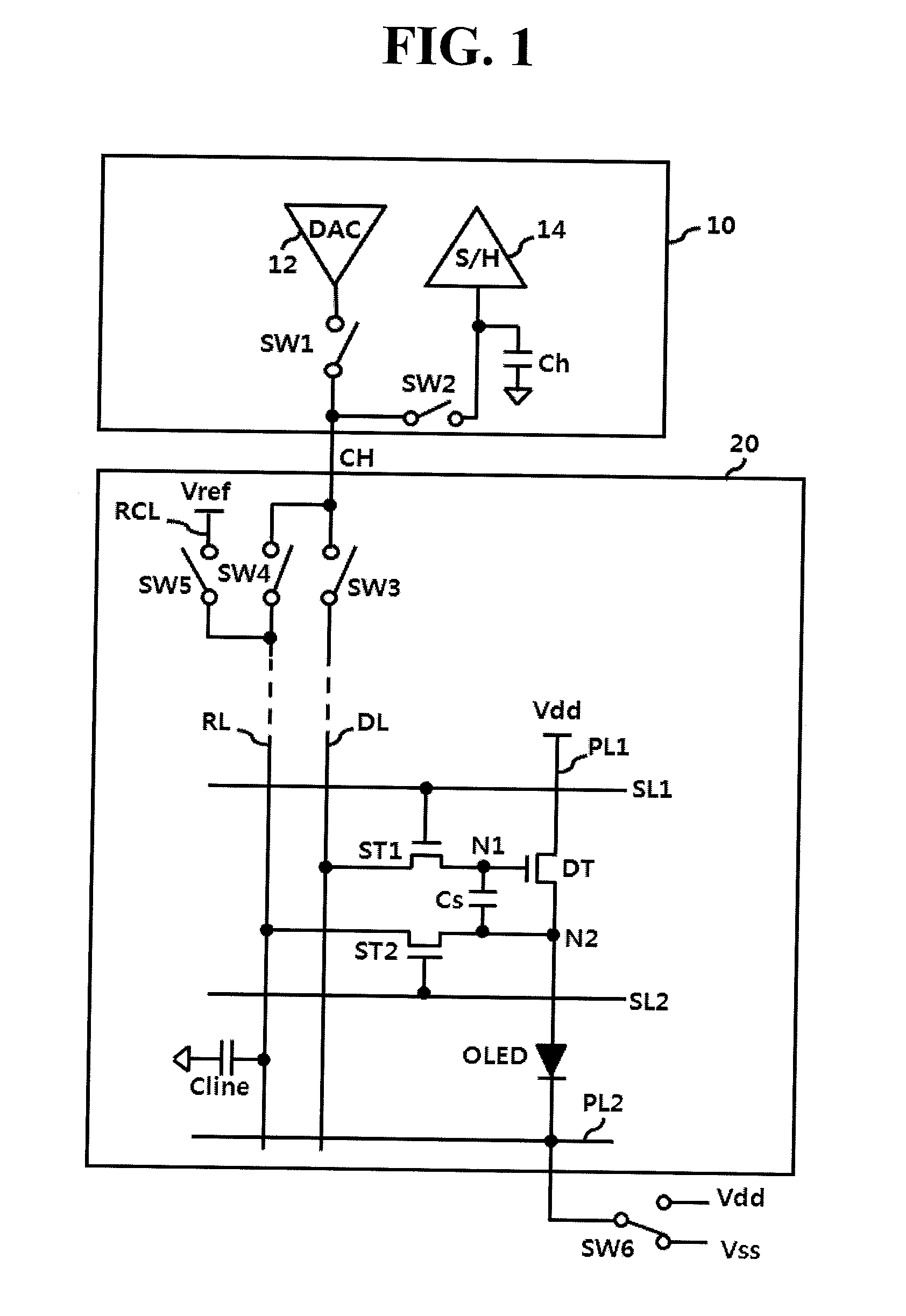
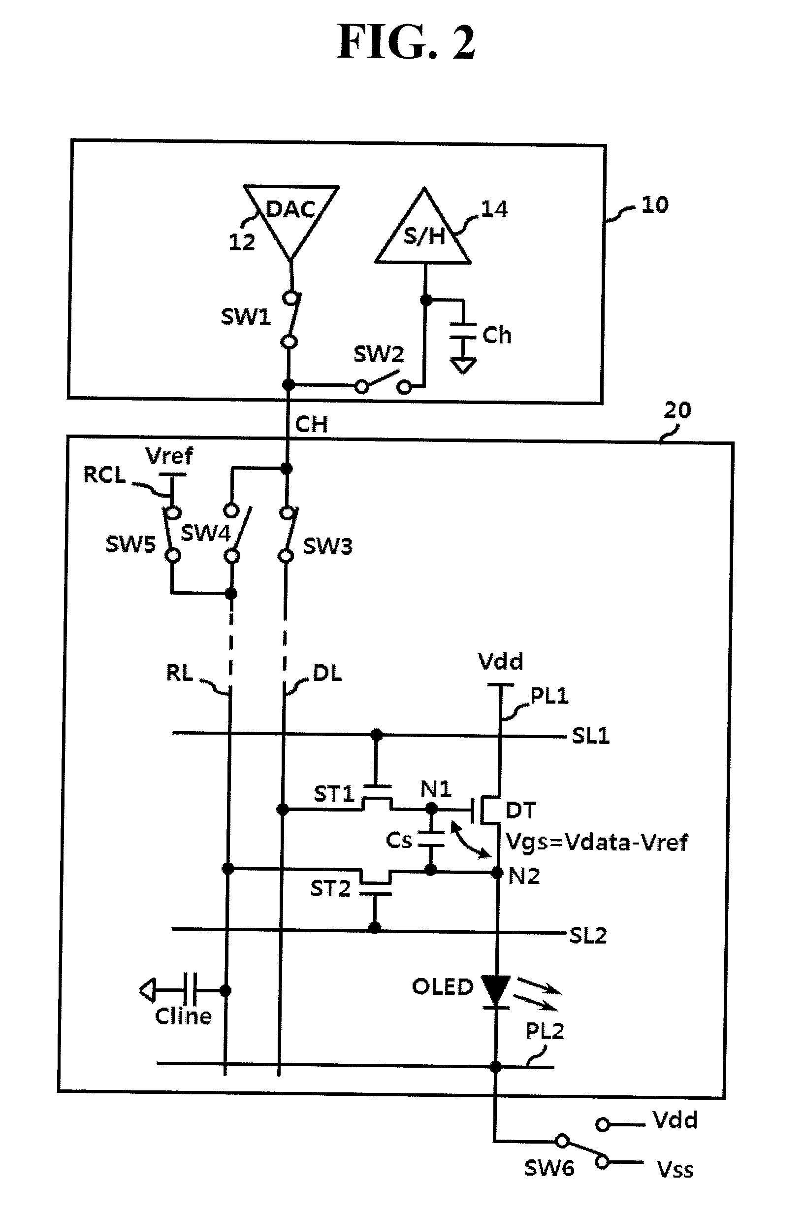
[0072]FIG. 1 is an equivalent circuit diagram illustrating a partial configuration of an OLED display device for pixel current sensing according to a first exemplary embodiment of the present invention.

[0073]The OLED display device illustrated in FIG. 1 includes a display panel 20 in which a pixel array is formed and a data driver 10 for driving a data line DL through an output channel CH connected to the display panel 20, sensing a current of each pixel at high speed, and outputting the sensing current. For convenience of description, the display panel 20 representatively shows the configuration of one pixel and the data driver 10 shows the configuration of a driver connected to the one output channel CH.

[0...


PUM


Abstract

An OLED display device which can sense a current of each pixel at high speed by a simple structure in order to compensate for luminance non-uniformity and a pixel current sensing method thereof are discussed. The OLED display device includes a display panel including pixels, each including a light emitting element and a pixel circuit for independently driving the light emitting element, a data driver for driving a data line connected to the pixel circuit using a data voltage, floating one of the data line, a reference line for supplying a reference voltage to the pixel circuit, and a power line for supplying a power to the pixel circuit to use the floated line as a current sensing line, sensing a voltage corresponding to a pixel current of the pixel circuit flowing to the current sensing line, and outputting the sensing voltage, in a sensing mode.

Description

[0001]This application claims the benefit of Korean Patent Application No. 10-2011-0087396, filed on Aug. 30, 2011, and Korean Patent Application No. 10-2012-0079801, filed on Jul. 23, 2012,which are hereby incorporated by reference as if fully set forth herein.BACKGROUND OF THE INVENTION[0002]1 Field of the Invention[0003]The present invention relates to an Active Matrix Organic Light Emitting Diode (AMOLED) display device, and more particularly, to an AMOLED display device which can sense a current of each pixel at high speed by a simple structure in order to compensate for a luminance deviation between pixels and a pixel current sensing method thereof.[0004]2. Discussion of the Related Art[0005]An AMOLED display device is a self-luminous element in which an organic light emitting layer emits light by recombination of electrons and holes and is expected to be used as a future generation display device due to high luminescence, a low driving voltage, and ultra thin thickness.[0006]...

Claims


Application Information

Patent Timeline
Patent Type & Authority Applications(United States)
IPC IPC(8): G09G5/10G09G3/30
CPCG09G3/3291G09G2320/045G09G2320/0693G09G2320/043G09G2300/0866G09G2320/0295G09G3/3233G09G5/18
Inventor MIZUKOSHI, SEIICHI
Owner LG DISPLAY CO LTD
Why Eureka
Try Eureka