Image correction device and image correction method

a technology of image correction and image luminance, which is applied in the field of image correction, can solve the problems of inability to solve the color-shift problem occurring in such areas of the image, the generation of peripheral shading of an image, and the local color-shifting problem of some images, so as to achieve the effect of improving the evenness of image luminan

Active Publication Date: 2013-02-28
NOVATEK MICROELECTRONICS CORP
View PDF6 Cites 3 Cited by
  • Summary
  • Abstract
  • Description
  • Claims
  • Application Information

AI Technical Summary

Benefits of technology

[0009]The invention is directed to an image correction device, which is capable of adjusting a distribution of gain values by transforming coordinates and providing correction parameters of different directions according to the transformed coordinates, so as to effectively improve evenness of image luminance. Moreover, the

Problems solved by technology

In a general image input/output device, intensity of light received by a lens can be different due to different distances between the light and a lens center, and since a typical image sensing device generally has a shape of rectangle, a problem of peripheral shading of an image is generated.
However, the lens shading correction method is only used to balance luminance of the central and peripheral areas of an image, incapable of resolving the color-shift problem occurring in such areas of the image.
Moreover, the local color-shifting problem for some images are caused not only by lens of the image input/output device, but by different combinations of systems or sensing devices.
Accordingly, adjusting the lens cannot completely resolve the color-shift problem.
Regarding the AWB method, it ca

Method used


Image

  • Image correction device and image correction method
  • Image correction device and image correction method
  • Image correction device and image correction method

Examples


Embodiment Construction

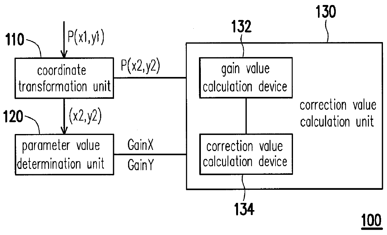
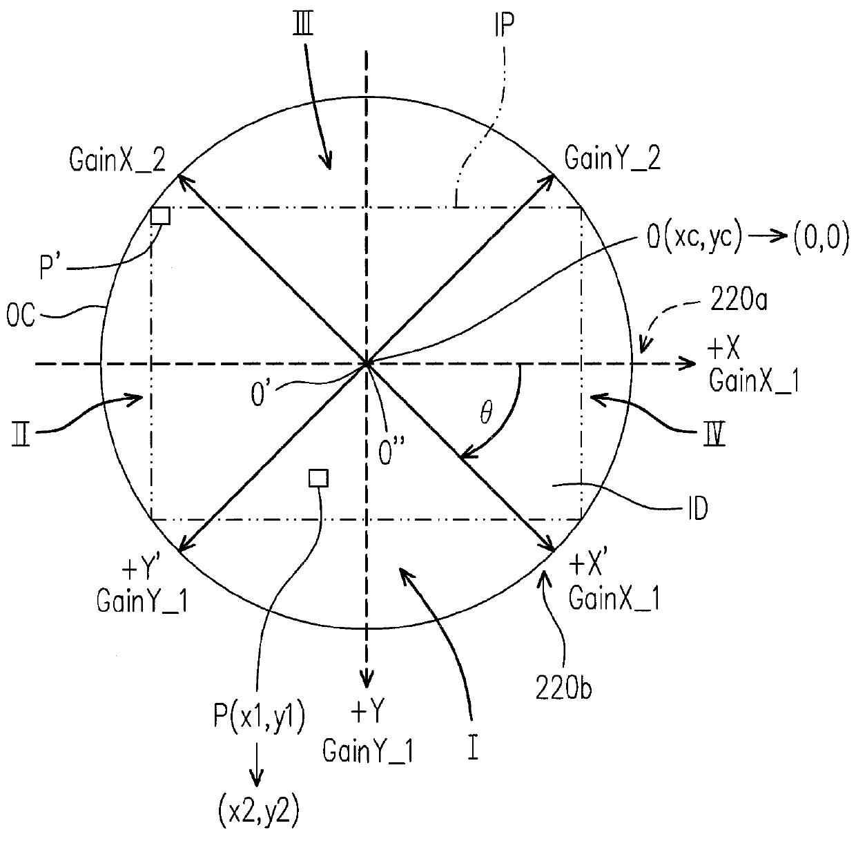
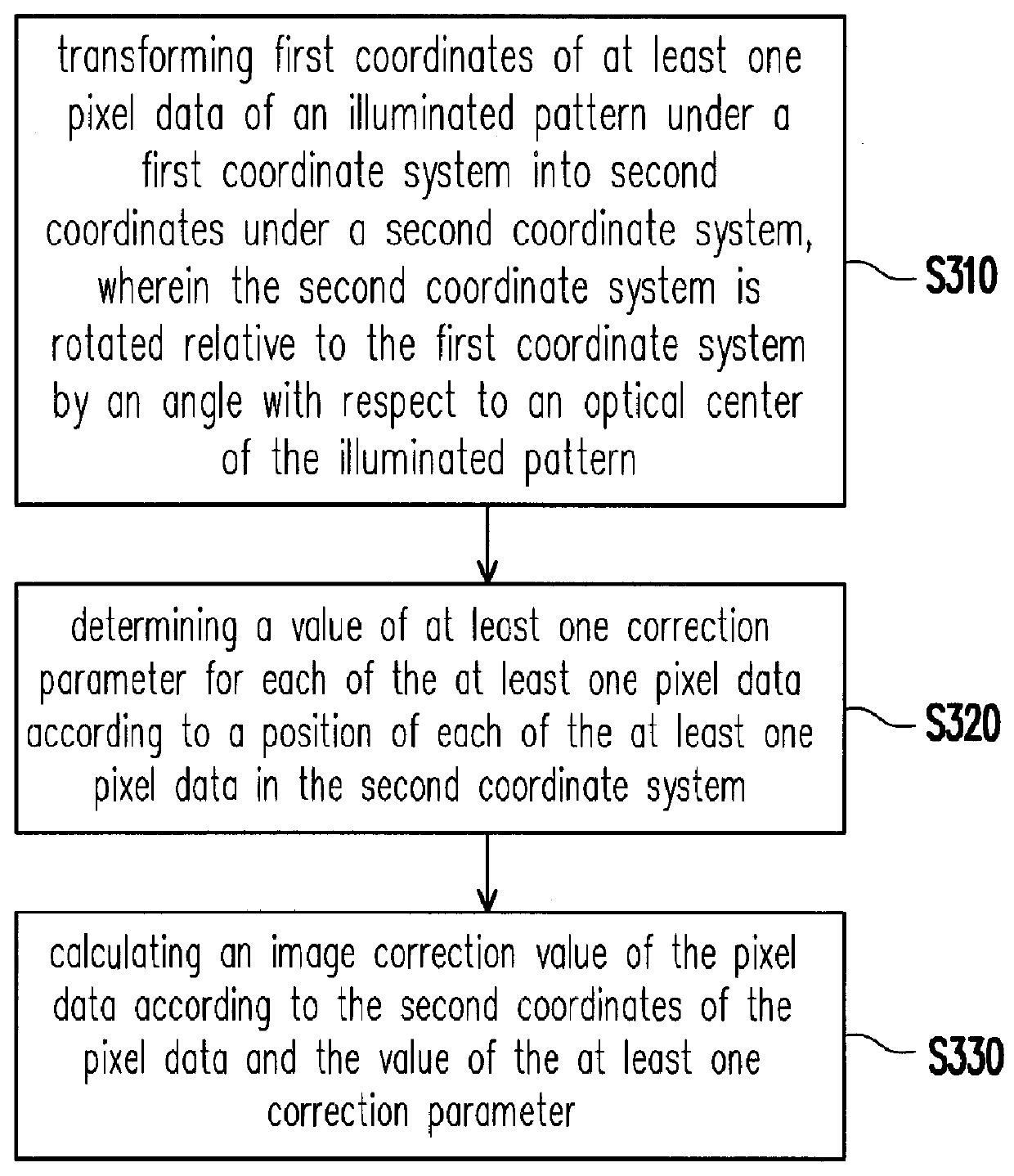
[0026]FIG. 1 is a structural block diagram of an image correction device 100 according to an embodiment. FIG. 2 is a schematic diagram of a first coordinate system and a second coordinate system according to an embodiment, introducing how the image correction device 100 corrects pixel data. A detailed structure and an operation mechanism of the image correction device 100 of the present embodiment are introduced below with reference of FIG. 1 and FIG. 2.

[0027]As shown in FIG. 1, the image correction device 100 includes a coordinate transformation unit 110, a parameter value determination unit 120, and a correction value calculation unit 130.

[0028]The coordinate transformation unit 110 receives first coordinates (x1, y1) of at least one pixel data P of an illuminated pattern OC under a first coordinate system 220a, and transforms the first coordinates (x1, y1) into second coordinates (x2, y2) under a second coordinate system 220b, which is rotated relative to the first coordinate sys...


PUM


Abstract

An image correction device includes a coordinate transformation unit, a parameter value determination unit, and a correction value calculation unit. The coordinate transformation unit receives first coordinates of at least one pixel data of an illuminated pattern under a first coordinate system, and transforms the first coordinates into second coordinates under a second coordinate system, wherein the second coordinate system is rotated relative to the first coordinate system by an angle with respect to an optical center of the illuminated pattern. The parameter value determination unit determines a respective value of at least one correction parameter according to the position of each of the at least one pixel data in the second coordinate system. The correction value calculation unit calculates an image correction value of each of the at least one pixel data according to the second coordinates and the respective value of the at least one correction parameter.

Description

BACKGROUND OF THE INVENTION[0001]1. Field of the Invention[0002]The invention relates to image correction. Particularly, the invention relates to an image correction device and an image correction method.[0003]2. Description of Related Art[0004]In a general image input / output device, intensity of light received by a lens can be different due to different distances between the light and a lens center, and since a typical image sensing device generally has a shape of rectangle, a problem of peripheral shading of an image is generated. A lens shading correction method is used to correct or compensate the peripheral shading. Generally, such method is to obtain a luminance variation curve of the lens by directly disposing the lens of the image input / output device in front of a parallel-light generating machine, and correct luminance unevenness of the lens center and the periphery thereof according to the luminance variation curve.[0005]Moreover, many image input / output devices have an au...

Claims


Application Information

Patent Timeline
IPC IPC(8): H04N5/217G06K9/40
CPCG06T5/006H04N5/2176H04N25/63
Inventor HSU, WEI
Owner NOVATEK MICROELECTRONICS CORP
Why Eureka
Try Eureka