
A/d converter and solid-state imaging apparatus

a converter and solid-state imaging technology, applied in the field of a/d converters and solid-state imaging apparatuses, can solve the problems of adversely affecting the output of each comparator, etc., and achieve the effect of simple arrangement and complicated circuit arrangement of a/d converters

Inactive Publication Date: 2013-03-21
CANON KK
View PDF0 Cites 18 Cited by
  • Summary
  • Abstract
  • Description
  • Claims
  • Application Information

AI Technical Summary

Benefits of technology

The patent text describes a technique to correct the output of a comparator in an A / D converter. The technique uses a controller to feedback the output of the comparator back into its input, which causes complicated circuit arrangement and noise. The invention aims to provide a simpler solution to correct the offset voltage of the comparator. The technical effect of the invention is to improve the accuracy and reliability of the A / D converter.

Problems solved by technology

For this reason, the circuit arrangement of the A / D converter is complicated, and noise caused by the controller adversely influences the output of each comparator.

Method used


Image

  • A/d converter and solid-state imaging apparatus
  • A/d converter and solid-state imaging apparatus
  • A/d converter and solid-state imaging apparatus

Examples


Embodiment Construction

[0017]An embodiment of the present invention will be described hereinafter with reference to the accompanying drawings. The same reference numerals denote the same components throughout the drawings, and a repetitive description thereof will be avoided.

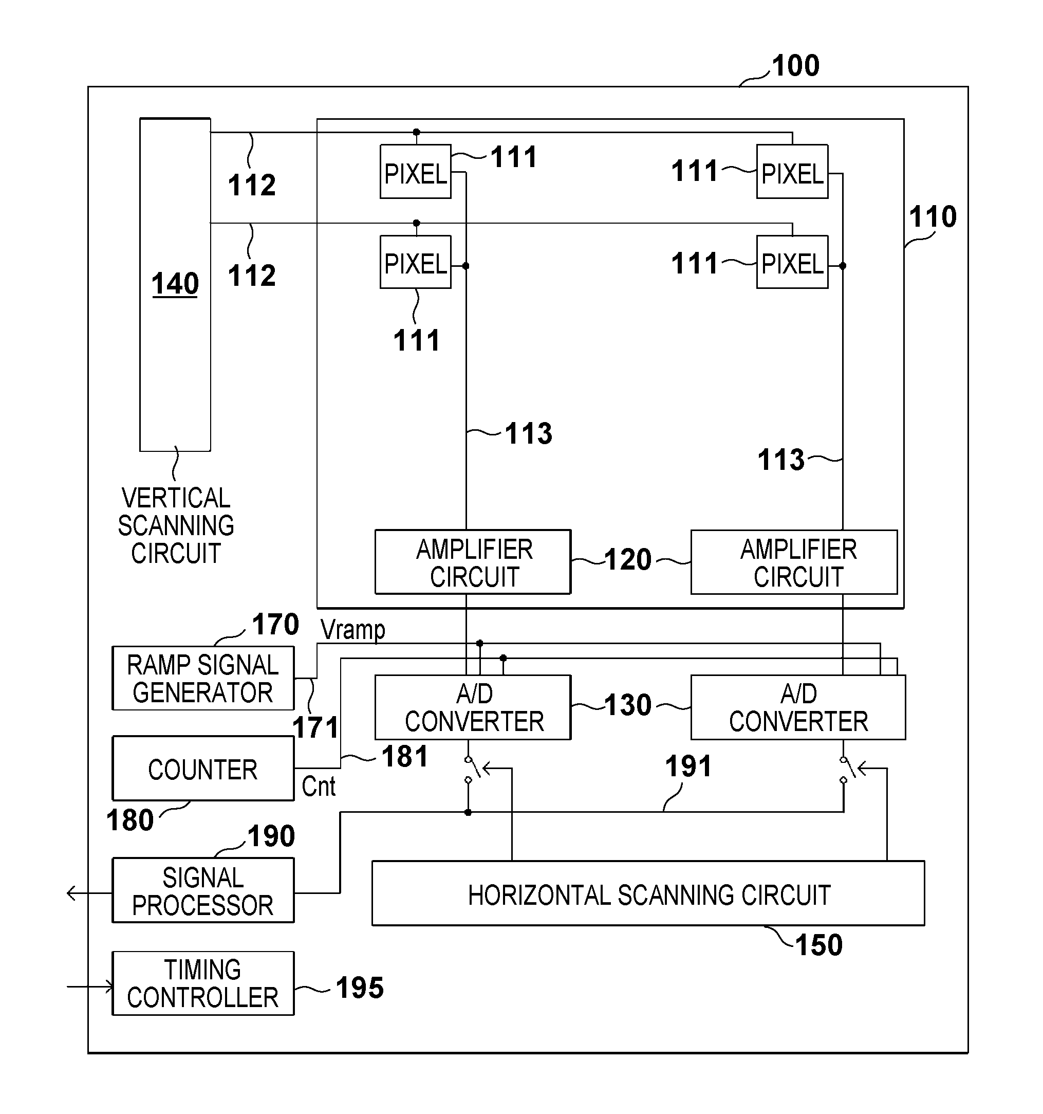
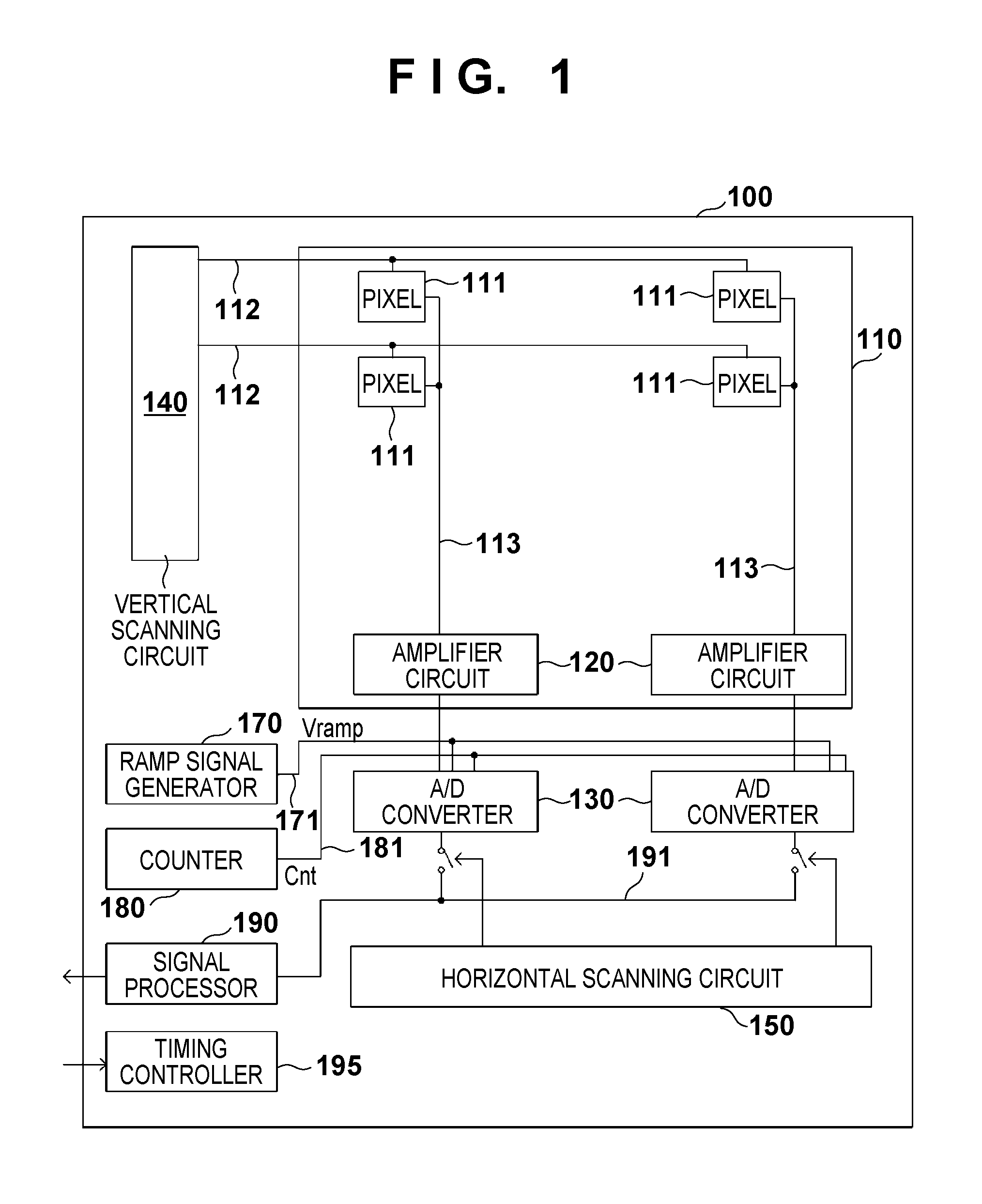
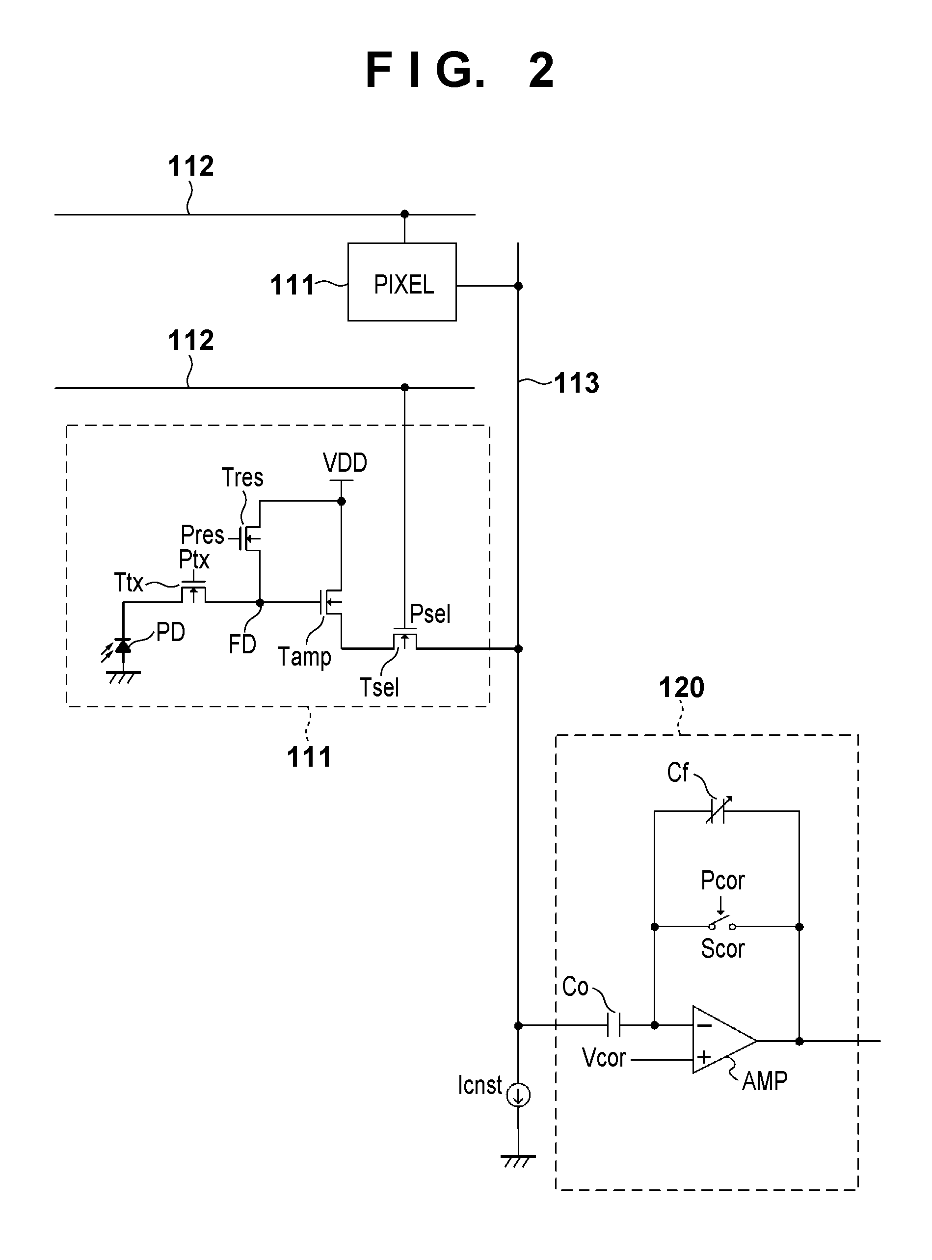
[0018]An example of a schematic arrangement of a solid-state imaging apparatus 100 according to one embodiment of the present invention will be described below with reference to FIG. 1. The solid-state imaging apparatus 100 is, for example, a CMOS image sensor, which photoelectrically converts incoming light indicating an object image, and externally outputs an electrical signal obtained by the photoelectric conversion as digital data. The solid-state imaging apparatus 100 can include an analog signal generator 110 including a pixel array formed by arranging a plurality of pixels 111 in a matrix. FIG. 1 illustrates four pixels 111 for the sake of simplicity, but the number of pixels 111 is not limited to this. Each pixel 111 photoelec...


PUM


Abstract

Provided is an A / D converter including an input terminal, a reference signal line for supplying a reference signal which changes temporally, a comparator, a correction capacitor connected to an inverting input terminal of the comparator; and an output circuit which outputs digital data corresponding to an analog signal input to the input terminal. In a first state in which a total voltage of a first analog signal and an offset voltage of the comparator is held in the correction capacitor, a second analog signal input to the input terminal is supplied to a non-inverting input terminal of the comparator, and the second analog signal or the total voltage is changed using the reference signal, thereby outputting, from the output circuit, digital data.

Description

BACKGROUND OF THE INVENTION[0001]1. Field of the Invention[0002]The present invention relates to an A / D converter and solid-state imaging apparatus.[0003]2. Description of the Related Art[0004]A technique which arranges A / D converters in correspondence with columns of pixels arranged in an array and converts signals from the respective pixels into digital data in a solid-state imaging apparatus is known. However, since offset voltages of comparators included in the respective A / D converters are different, an A / D conversion period has to be set in consideration of a maximum value of the offset voltages. U.S. Pat. No. 7,671,908 has proposed a technique for correcting an offset voltage by feeding back an output of the comparator included in each individual A / D converter to an input of that comparator.SUMMARY OF THE INVENTION[0005]The technique of U.S. Pat. No. 7,671,908 uses a controller to feed back the output of the comparator to its input. For this reason, the circuit arrangement of...

Claims


Application Information

Patent Timeline
Patent Type & Authority Applications(United States)
IPC IPC(8): H03M1/12H01L27/146H04N25/65
CPCH04N5/37455G02F7/00H04N5/378H04N25/78H04N25/75H04N25/772
Inventor NAKAMURA, KOHICHIHIYAMA, HIROKIITANO, TETSUYASAITO, KAZUHIRO
Owner CANON KK
Learn More