Voltage regulator

a voltage regulator and voltage regulation technology, applied in the direction of electric variable regulation, process and machine control, instruments, etc., can solve the problems of increasing the undershoot or overshoot of the output voltage vout in the load transient response, and achieve the effect of improving the transient response characteristics

Active Publication Date: 2013-03-21
ABLIC INC
View PDF10 Cites 18 Cited by
  • Summary
  • Abstract
  • Description
  • Claims
  • Application Information

AI Technical Summary

Benefits of technology

[0014]The present invention has been provided in view of the above problem. Therefore, it is an object of the present invention to provide a voltage regulator having good transient response characteristics and capable of maintaining stable operation.
[0017]The output of the MOS transistor which constitutes the third source ground amplifier circuit is connected to the gate of the output MOS transistor without passing through a resistor. This enables the gate of the output MOS transistor to be controlled without delay. Therefore, even though a voltage three-stage amplifier circuit having a phase compensation circuit is used, the gate of the output MOS transistor is controllable without passing through the resistor of the phase compensation circuit, which enables an improvement of transient response characteristics.

Problems solved by technology

The delay in charging and discharging the parasitic capacitance of the MOS transistor 114 causes a problem of increasing the undershoot or overshoot of the output voltage Vout in a load transient response.

Method used


Image

  • Voltage regulator
  • Voltage regulator
  • Voltage regulator

Examples


first embodiment

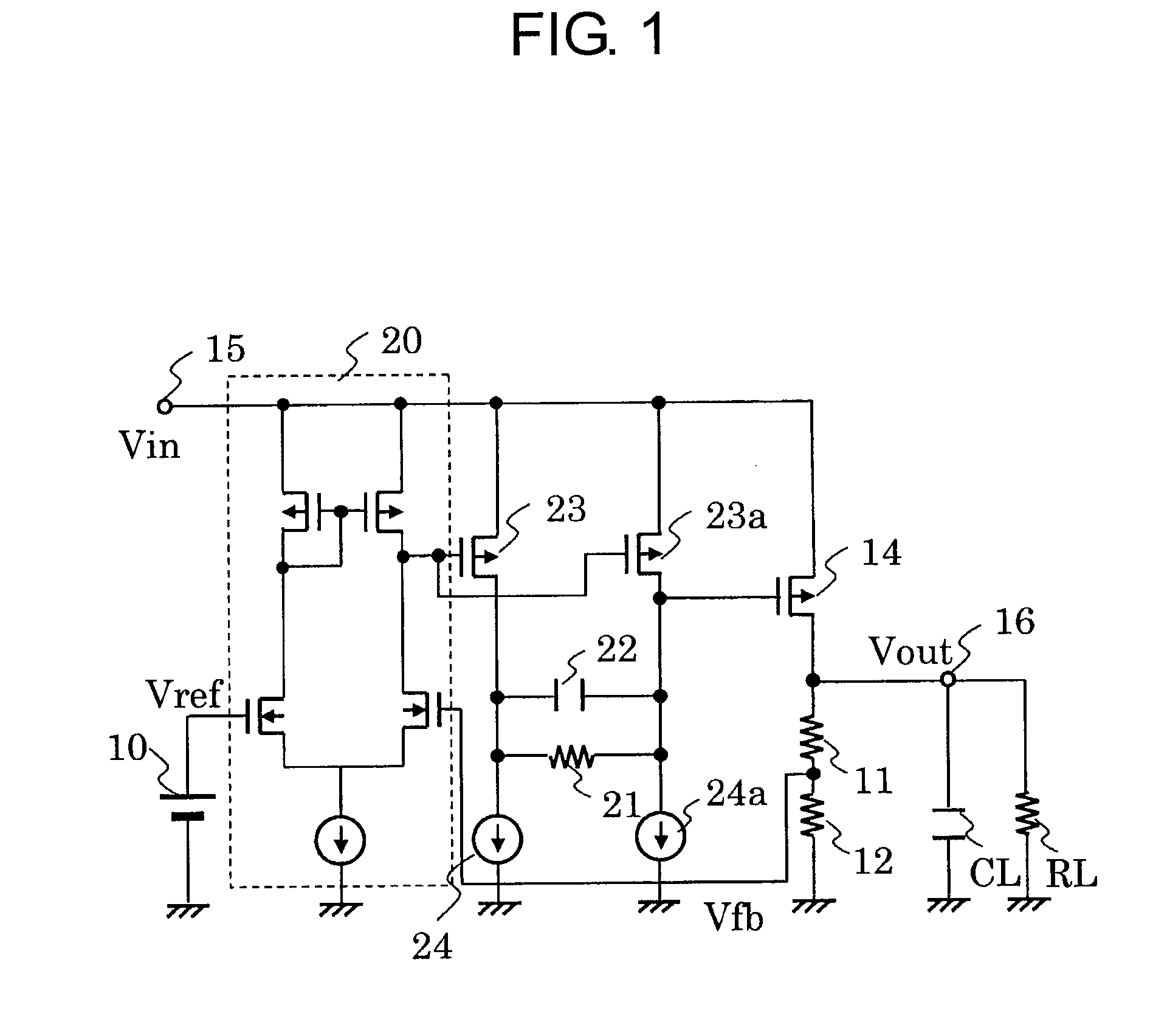
[0025]Referring to FIG. 1, there is provided a circuit diagram of a voltage regulator according to a first embodiment.

[0026]The voltage regulator according to the first embodiment includes a reference voltage circuit 10, a differential amplifier 20, MOS transistors 23 and 23a, constant current sources 24 and 24a, a resistor 21, a capacitor 22, a MOS transistor 14, which is an output MOS transistor, and bleeder resistors 11 and 12.

[0027]The bleeder resistors 11 and 12 generate a feedback voltage Vfb by dividing an output voltage Vout of an output terminal 16. The differential amplifier 20 compares a reference voltage output from the reference voltage circuit 10 with the feedback voltage Vfb. An output of the differential amplifier 20 is input to a gate terminal of the MOS transistor 23 constituting a first source ground amplifier circuit and to a gate terminal of the MOS transistor 23a constituting a third source ground amplifier circuit. The MOS transistor 23 has a source terminal, ...

second embodiment

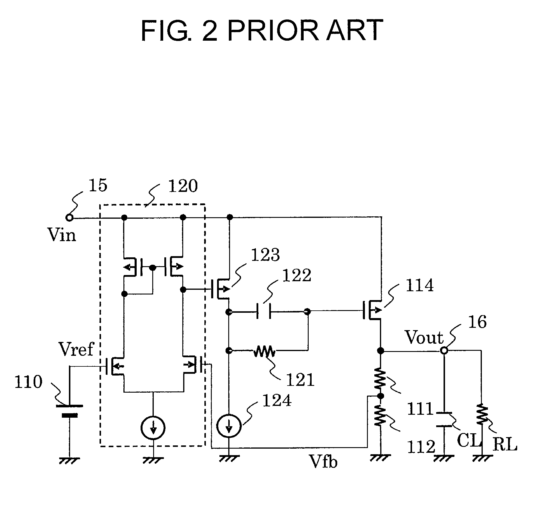
[0041]FIG. 3 is a circuit diagram of a voltage regulator according to a second embodiment. The voltage regulator according to the second embodiment has an output load current detection circuit 30 which senses an output load current. Moreover, the constant current source 24a additionally has a switch circuit and a constant current source which are sequentially connected. The circuit configuration is the same as in the first embodiment except the output load current detection circuit 30 and the constant current source 24a.

[0042]The output load current detection circuit 30 has a terminal for outputting a detection signal connected to a switch circuit of the constant current source 24a. Further, the output load current detection circuit 30 switches the current value of the constant current source 24a according to the detection signal.

[0043]For example, in the case of an increase in an output load current, the output load current detection circuit 30 increases the current value of the c...

third embodiment

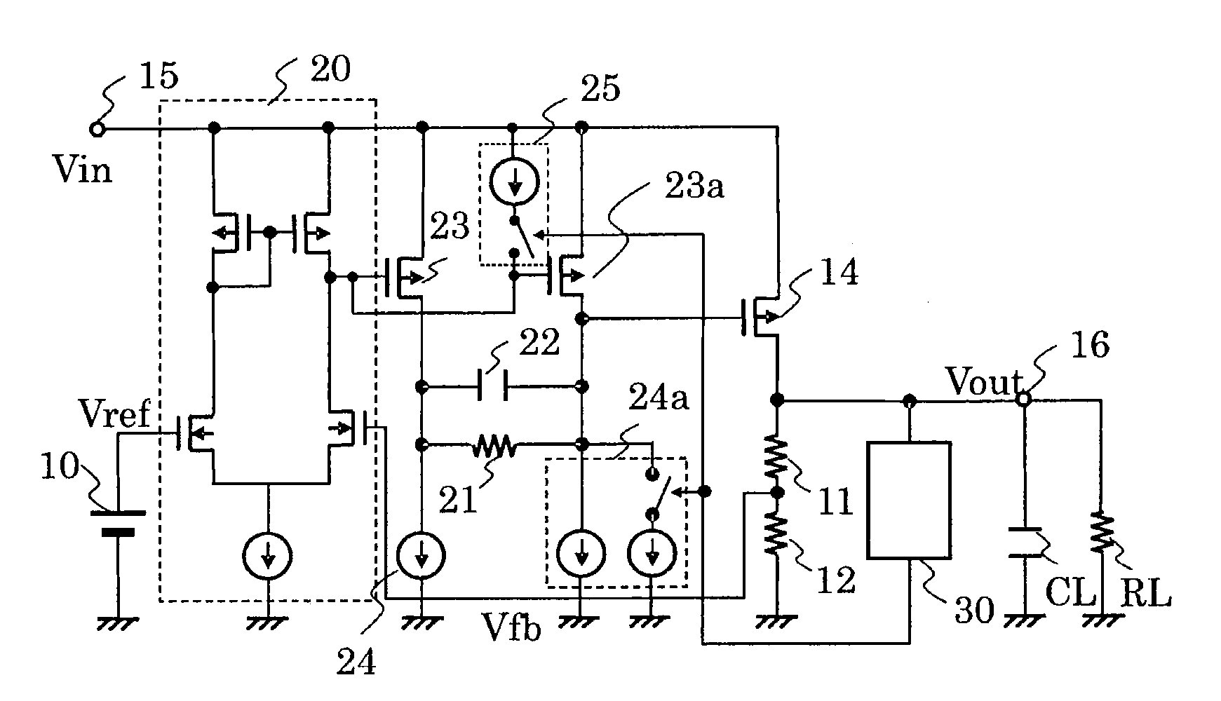
[0045]FIG. 4 is a circuit diagram of a voltage regulator according to a third embodiment.

[0046]The voltage regulator according to the third embodiment has an output load current detection circuit 30 which senses output load current. Moreover, the resistor 21 additionally has a switch circuit and a constant current source which are connected in parallel. The circuit configuration is the same as in the first embodiment except the output load current detection circuit 30 and the resistor 21.

[0047]The output load current detection circuit 30 has a terminal for outputting a detection signal connected to the switch circuit of the resistor 21. In addition, the output load current detection circuit 30 switches the resistance value of the resistor 21 according to the detection signal.

[0048]For example, in the case of an increase in an output load current, the output load current detection circuit 30 decreases the resistance value of the resistor 21. This enables the resistance value to be sw...


PUM


Abstract

A voltage regulator having good transient response characteristics and maintaining stable operation is provided. The voltage regulator includes: a first MOS transistor having a gate terminal connected to an output terminal of the differential amplifier circuit; a first constant current source provided between the first MOS transistor and a ground terminal; an output MOS transistor having a gate terminal connected to a drain terminal of the first MOS transistor via a phase compensation circuit; a second MOS transistor having a gate terminal to which an output of the differential amplifier circuit is input and a drain terminal connected to the gate terminal of the output MOS transistor; and a second constant current source provided between the second MOS transistor and a ground terminal.

Description

RELATED APPLICATIONS[0001]This application claims priority under 35 U.S.C. §119 to Japanese Patent Application Nos. 2011-201444 filed on Sep. 15, 2011 and 2012-156619 filed on Jul. 12, 2012, the entire content of which is hereby incorporated by reference.BACKGROUND OF THE INVENTION[0002]1. Field of the Invention[0003]The present invention relates to a voltage regulator which generates a constant output voltage Vout upon receiving an input voltage, and more specifically to transient response characteristics and stable operation of a voltage regulator.[0004]2. Description of the Related Art[0005]In general, a voltage regulator generates a constant output voltage Vout to an output terminal 16 upon receiving an input voltage Vin which is input to an input terminal 15. The voltage regulator supplies electric current in response to load fluctuations to maintain the output voltage Vout constant consistently.[0006]FIG. 2 is a circuit diagram of a conventional voltage regulator.[0007]A refer...

Claims


Application Information

Patent Timeline
Patent Type & Authority Applications(United States)
IPC IPC(8): G05F1/10
CPCG05F1/575G05F3/02G05F3/24
Inventor SUZUKI, TERUO
Owner ABLIC INC
Why Eureka
Try Eureka