Method for preparing a substrate by implantation and irradiation

a technology of substrate and irradiation, which is applied in the direction of basic electric elements, semiconductor/solid-state device manufacturing, electric apparatus, etc., can solve the problems of affecting the development of applications, and reducing the application range of epitaxy,

Active Publication Date: 2013-03-21
SOITEC SA
View PDF2 Cites 18 Cited by
  • Summary
  • Abstract
  • Description
  • Claims
  • Application Information

AI Technical Summary

Benefits of technology

[0024]Selective and adiabatic irradiation allows a reduction of the light budget needed for detachment of the buried layer.

Problems solved by technology

However, the development of these applications is slowed by the techno-economic limits of the substrates.
However, in the case of substrates made of III-N material, implantation requires doses of atomic or ionic species that are five to ten times greater than in silicon, which results in a considerably increased process cost.
This constitutes a major drawback, because the surface of the sacrificial layer is degraded by these treatments, so that it no longer has an optimal crystal matrix for epitaxy.

Method used


Image

  • Method for preparing a substrate by implantation and irradiation
  • Method for preparing a substrate by implantation and irradiation
  • Method for preparing a substrate by implantation and irradiation

Examples


Embodiment Construction

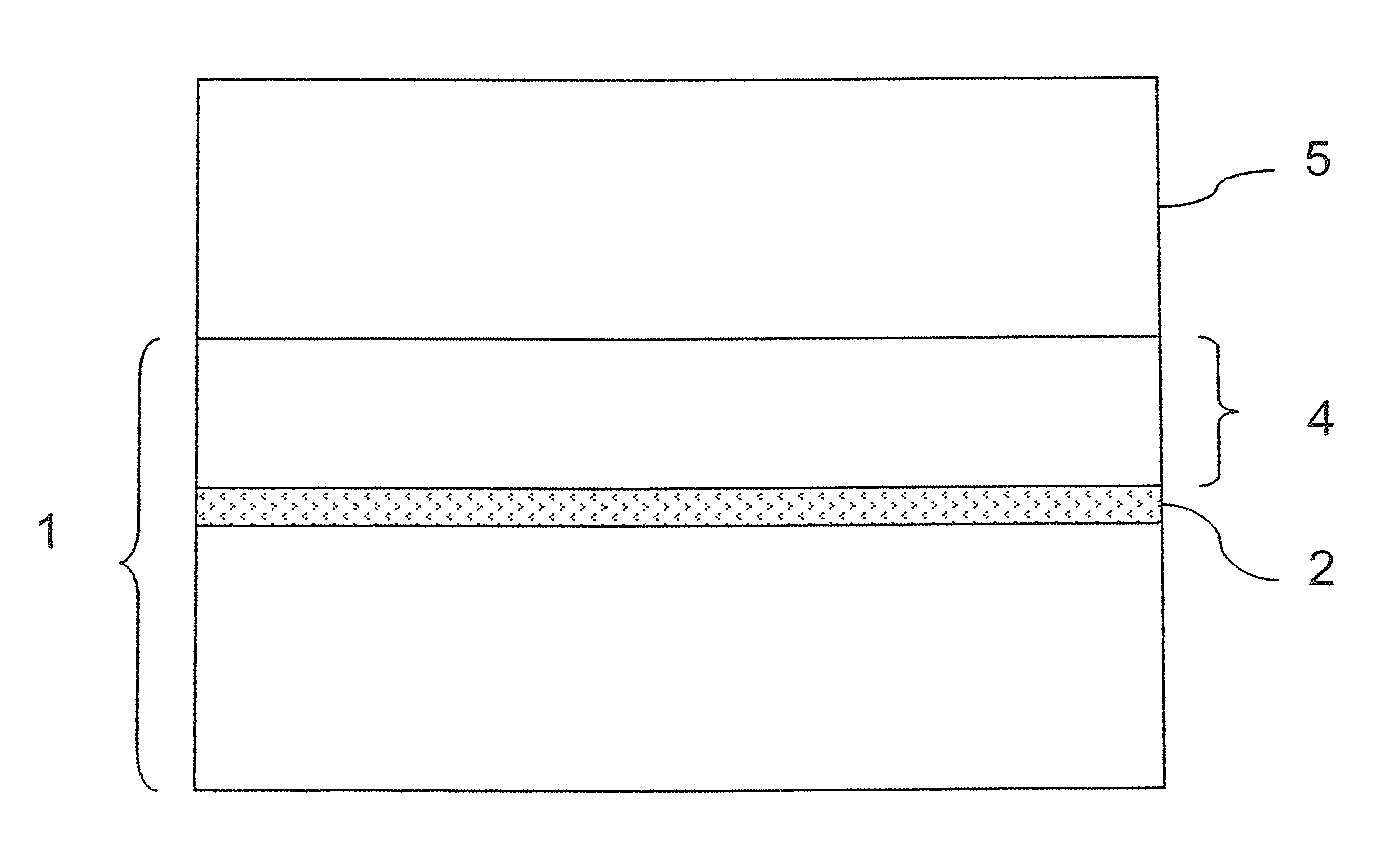
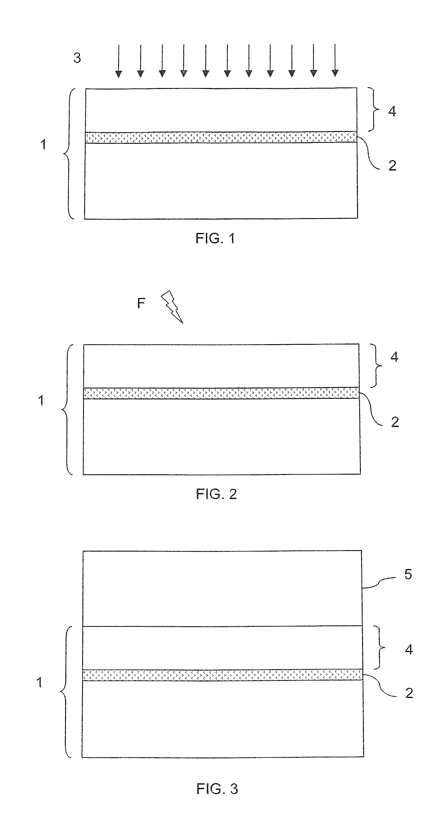
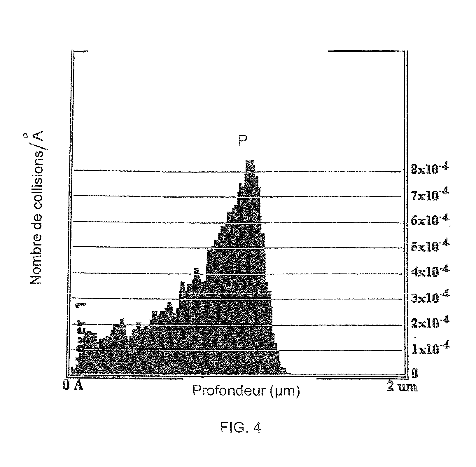
[0046]The invention applies to any substrate made of a compound material, crystalline or not, whose optical absorption properties (particularly the optical absorption coefficient within a given range of frequencies, or the imaginary part of the index of refraction) are capable of being modified within a localized zone by an implantation of particles. The compound material must also be capable of decomposing in this zone under the influence of an energy input by a light flux in and near this zone.

[0047]By “compound material” is meant a material made up of at least two elements.

[0048]By “decomposition” is meant an alteration of the fundamental structure of the material that can consist, depending on the material, of a phase separation, the creation of new phases, the creation of inclusions, etc.

[0049]Compound materials are materials made up of at least two types of atoms. Among said compound materials can be mentioned the III-V compound semiconductors in particular, and particularly t...


PUM


Abstract

A method for preparing a substrate for detaching a layer by irradiation of the substrate with a light flux for heating a buried region of the substrate and bringing about decomposition of the material of that region to detach said detachment layer. The method includes fabricating an intermediate substrate including a first buried layer, and a second covering layer that covers all or part of the first layer, with the covering layer being substantially transparent to the light flux and with the buried layer formed by implantation of particles into the substrate, followed by absorbing the flux, and selectively and adiabatically irradiating a treated region of the buried layer until at least partial decomposition of the material constituting it ensues.

Description

FIELD OF THE INVENTION[0001]The present invention relates to a method for preparing a substrate made of semiconductor materials, for the purpose of detaching a layer of said substrate.BACKGROUND OF THE INVENTION[0002]Semiconductors of the III-N type, that is having the general formula AlxGayIn1-x-yN where 0≦x≦1, 0≦y≦1 and x+y≦1, and GaN in particular, have characteristics which make them very attractive for the optoelectronic field, power components and radio frequency applications.[0003]However, the development of these applications is slowed by the techno-economic limits of the substrates.[0004]Indeed, device manufacturing depends generally on the transfer to a supporting substrate of a thin layer taken from a donor substrate, which is a massive substrate of high quality III-N material suited to the intended application.[0005]The Smart Cut™ process in particular is a well-known transfer technique, which consists generally of implanting a dose of atomic or ionic species into a dono...

Claims


Application Information

Patent Timeline
Patent Type & Authority Applications(United States)
IPC IPC(8): H01L21/762
CPCH01L21/762H01L21/76254
Inventor BRUEL, MICHEL
Owner SOITEC SA
Why Eureka
Try Eureka