Touch sensing apparatus and method of manufacturing the same

a technology of touch sensing apparatus and manufacturing method, which is applied in the direction of printed circuits, printed circuit details, instruments, etc., can solve the problems of high defect rate, high manufacturing cost, and large thickness of the touch panel, and achieve the effect of improving touch sensing accuracy and reducing defect ra

Inactive Publication Date: 2013-04-04
MELFAS
View PDF10 Cites 44 Cited by
  • Summary
  • Abstract
  • Description
  • Claims
  • Application Information

AI Technical Summary

Benefits of technology

[0014]An advantage of the present invention is to provide a touch sensing apparatus having improved touch sensing accuracy and a method of manufacturing the same.
[0015]Another advantage of the present invention is to provide a touch sensing apparatus whose actual sensing region is increased for a given number of electrode channels disposed in a touch sensing panel and a method of manufacturing the same.
[0016]Another advantage of the present invention is to provide a touch sensing apparatus having a reduced defect rate during the formation of wiring patterns and a method of manufacturing the same.
[0017]Additional features and advantages of the invention will be set forth in the description which follows, and in part will be apparent from the description, or may be learned by practice of the invention. These and other advantages of the invention will be realized and attained by the structure particularly pointed out in the written description and claims hereof as well as the appended drawings.
[0018]To achieve these and other advantages and in accordance with the purpose of the present invention, as embodied and broadly described, a touch sensing apparatus having a transparent substrate that includes a touch sensing region and a peripheral region outside the tou...

Problems solved by technology

The touch panel including the drive electrode traces and the sense electrode traces under the drive electrode traces has drawbacks of a high manufacturing cost and a large thickness.
These drawbacks are at...

Method used


Image

  • Touch sensing apparatus and method of manufacturing the same
  • Touch sensing apparatus and method of manufacturing the same
  • Touch sensing apparatus and method of manufacturing the same

Examples


Embodiment Construction

[0034]Reference will now be made in detail to exemplary embodiments of the present invention, examples of which are illustrated in the accompanying drawings.

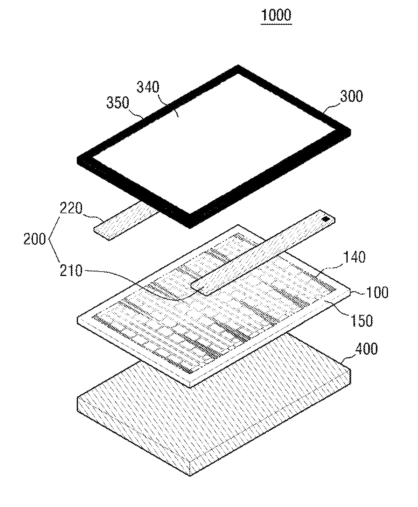
[0035]FIG. 1 is an exploded perspective view of a touch sensing apparatus 1000 according to an embodiment of the present invention.

[0036]Referring to FIG. 1, the touch sensing apparatus 1000 includes a transparent substrate 100, a circuit board 200 including a first circuit board 210 and a second circuit board 220, and a transparent window 300. The transparent substrate 100 may be made of a high-strength material such as toughened glass, acrylic resin or a hard material applicable to flexible displays, such as polyethylene terephthalate (PET), polycarbonate (PC), polyethersulfone (PES), polyimide (PI) or polymethly methacrylate (PMMA).

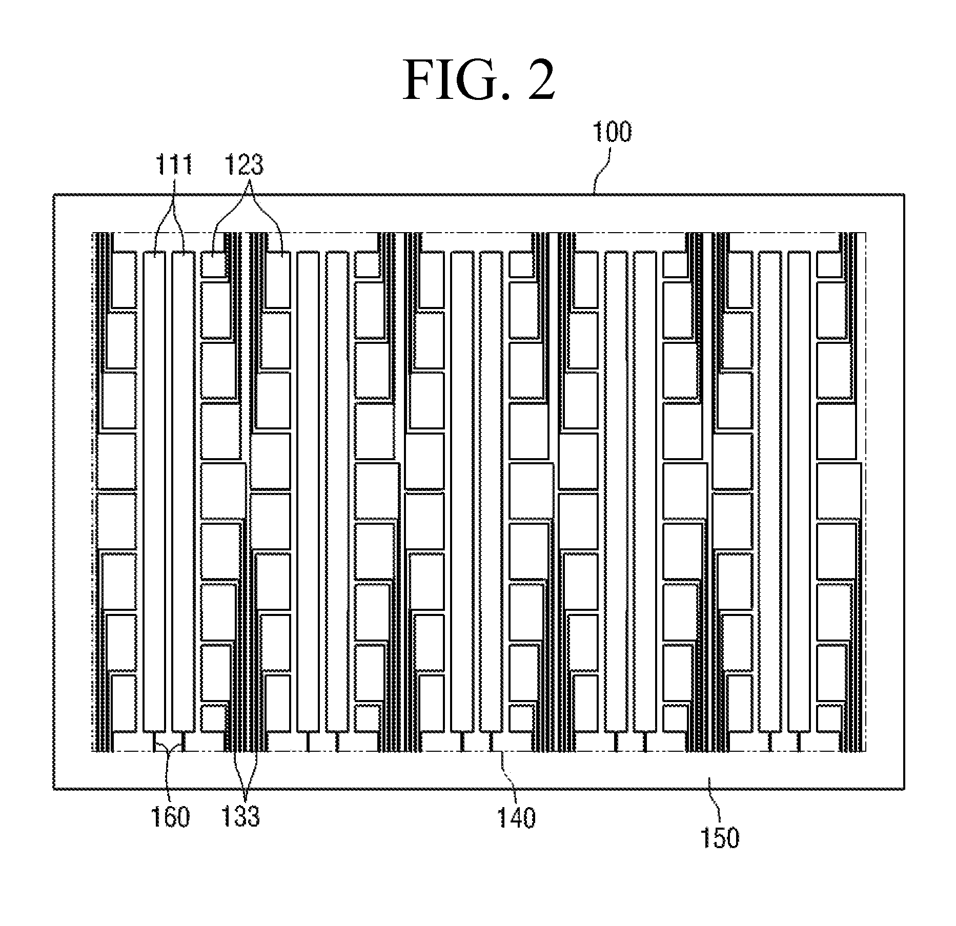
[0037]The transparent substrate 100 includes a touch sensing region 140 and a peripheral region 150. The touch sensing region 140 is a region that senses input information generated by a user's tou...


PUM

PropertyMeasurementUnit
Temperatureaaaaaaaaaa
Shapeaaaaaaaaaa

Abstract

Disclosed is a touch sensing apparatus having a transparent substrate that includes a touch sensing region and a peripheral region outside the touch sensing region. The touch sensing region may include a pair of column electrodes extending in a vertical direction; a plurality of patch electrodes arranged in two columns in the vertical direction, the two columns of patch electrodes interposed between the pair of column electrodes without an intervening column electrode; a plurality of first wirings electrically connected to the pair of column electrodes; and a plurality of second wirings electrically connected to the two columns of patch electrodes.

Description

CROSS-REFERENCE TO RELATED APPLICATIONS[0001]This application claims the benefit of Korean Patent Application Nos. 10-2011-0100368, filed on Sep. 30, 2011, and 10-2011-0121807, filed on Nov. 21, 2011, which are hereby incorporated by reference for all purposes as if fully set forth herein.BACKGROUND OF THE INVENTION[0002]1. Field of the Invention[0003]The present invention relates to a touch sensing apparatus and a method of manufacturing the same, and more particularly, to a touch sensing apparatus which has improved touch sensing accuracy and uses separate circuit boards, and a method of manufacturing the same.[0004]2. Discussion of the Related Art[0005]A touch sensing apparatus recognizes a user's screen touch or gesture as input information. Touch panels of touch sensing apparatuses are classified into resistive, capacitive, ultrasonic, and infrared touch panels according to their driving method. Of these touch panels, capacitive touch panels are drawing much attention due to ea...

Claims


Application Information

Patent Timeline
IPC IPC(8): H05K1/11H05K13/00
CPCG06F3/044Y10T29/49117G06F2203/04103G06F3/04164G06F3/0443G06F3/0448
Inventor KIM, JAE HONGNAM, SUNG II
Owner MELFAS
Why Eureka
Try Eureka