Multi-patterning lithography aware cell placement in integrated circuit design

a multi-patterning lithography and integrated circuit technology, applied in the field of multi-patterning lithography aware cell placement in integrated circuit design, can solve the problems of wiring limitations, complex designs produced and manipulated using these software tools

Inactive Publication Date: 2013-04-04
GLOBALFOUNDRIES INC
View PDF1 Cites 34 Cited by
  • Summary
  • Abstract
  • Description
  • Claims
  • Application Information

AI Technical Summary

Problems solved by technology

The designs produced and manipulated using these software tools are complex, often including millions of such components interconnected to form an intended electronic circuitry.
Placement problem is the problem of placing the cells of a chip such that the design

Method used


Image

  • Multi-patterning lithography aware cell placement in integrated circuit design
  • Multi-patterning lithography aware cell placement in integrated circuit design
  • Multi-patterning lithography aware cell placement in integrated circuit design

Examples


Embodiment Construction

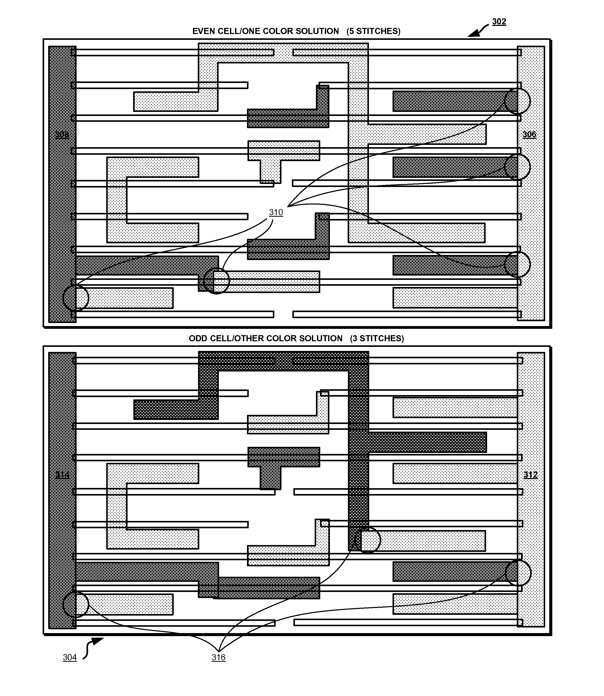
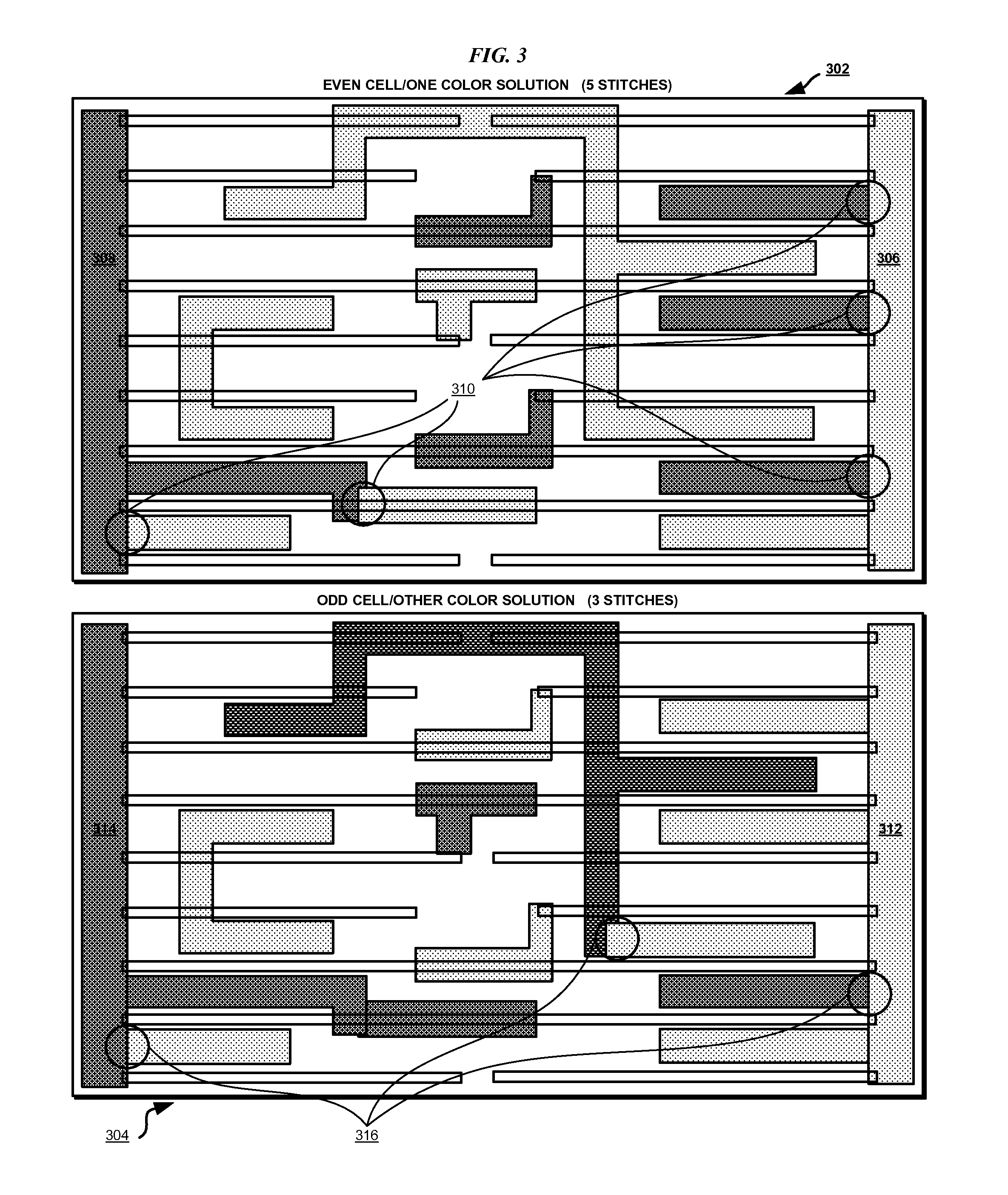
[0035]The IC designs are becoming increasingly complex, the number of components per design is increasing, and the size of components being printed is shrinking. The IC design process is being geared for producing components where the size of the components and inter-component spacing are fifteen (15) nanometer (nm) or less across. To give some perspective on the size of the components, the wavelength of the light used for lithography is approximately one hundred and ninety three (193) nm.

[0036]Multi-patterning lithography is a method to make sure the geometry printed on wafer has similar shapes and electrical properties as drawn on the mask, such as for the fifteen nm and smaller design technology, where a single mask is not sufficient to guarantee the printability of the design. Generally in MPL, the cells in the design are colored in different colors, each color forming a pattern and representing one exposure. In so dividing the shapes in the cells into different colors, the colo...


PUM


Abstract

A method, system, and computer program product for multi-patterning lithography (MPL) aware cell placement in integrated circuit (IC) design are provided in the illustrative embodiments. A global phase of cell movement is performed. A local phase cell movement is performed, wherein the local phase includes moving a color instance of the cell from a plurality of color instances of the cell within a row of cell in the IC design, wherein the global phase and the local phase are each performed before a final placement is produced for the IC design.

Description

RELATED APPLICATION[0001]The present invention is related to similar subject matter of co-pending and commonly assigned U.S. patent application Ser. No. 12 / 796,501 (Attorney Docket No. AUS920100139US1) entitled “DETAILED ROUTABILITY BY CELL PLACEMENT,” filed on Jun. 8, 2010, and U.S. patent application Ser. No. 12 / 796,550 (Attorney Docket No. AUS920100233US1) entitled “POST-PLACEMENT CELL SHIFTING,” filed on Jun. 8, 2010, which are hereby incorporated by reference.BACKGROUND[0002]1. Technical Field[0003]The present invention relates generally to a method, system, and computer program product for designing an integrated circuit. More particularly, the present invention relates to a method, system, and computer program product for multi-patterning lithography (MPL) aware cell placement in integrated circuit (IC) design.[0004]2. Description of the Related Art[0005]Modern day electronics include components that use integrated circuits. Integrated circuits are electronic circuits formed ...

Claims


Application Information

Patent Timeline
IPC IPC(8): G06F17/50
CPCG06F2217/12G06F17/5072G06F2119/18G06F30/392Y02P90/02
Inventor AGARWAL, KANAK BEHARIALPERT, CHARLES JAYLI, ZHUONAM, GI-JOONVISWANATHAN, NATARAJAN
Owner GLOBALFOUNDRIES INC
Why Eureka
Try Eureka