Semiconductor package

a technology of semiconductor chips and semiconductor devices, applied in the field of semiconductor packages, can solve the problems of reducing limiting the performance of semiconductor chips, etc., and achieve the effect of improving reliability and durability

Active Publication Date: 2013-04-11
SAMSUNG ELECTRONICS CO LTD
View PDF14 Cites 28 Cited by
  • Summary
  • Abstract
  • Description
  • Claims
  • Application Information

AI Technical Summary

Benefits of technology

[0006]The present general inventive concept provides a semi

Problems solved by technology

A process of miniaturizing a semiconductor device is accompanied by limitations to increase the perfo

Method used


Image

  • Semiconductor package
  • Semiconductor package
  • Semiconductor package

Examples


Embodiment Construction

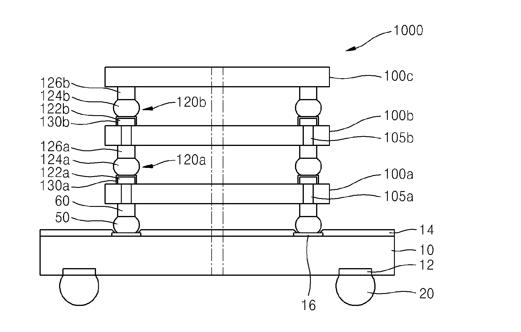
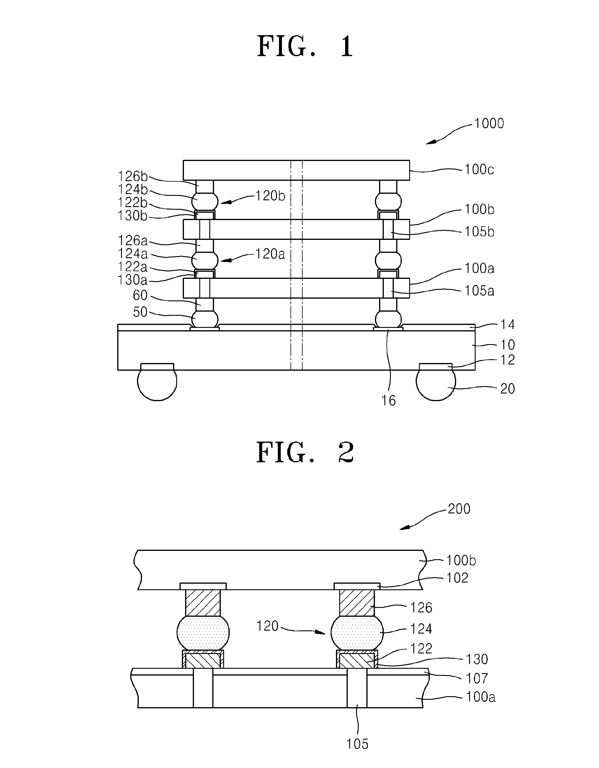
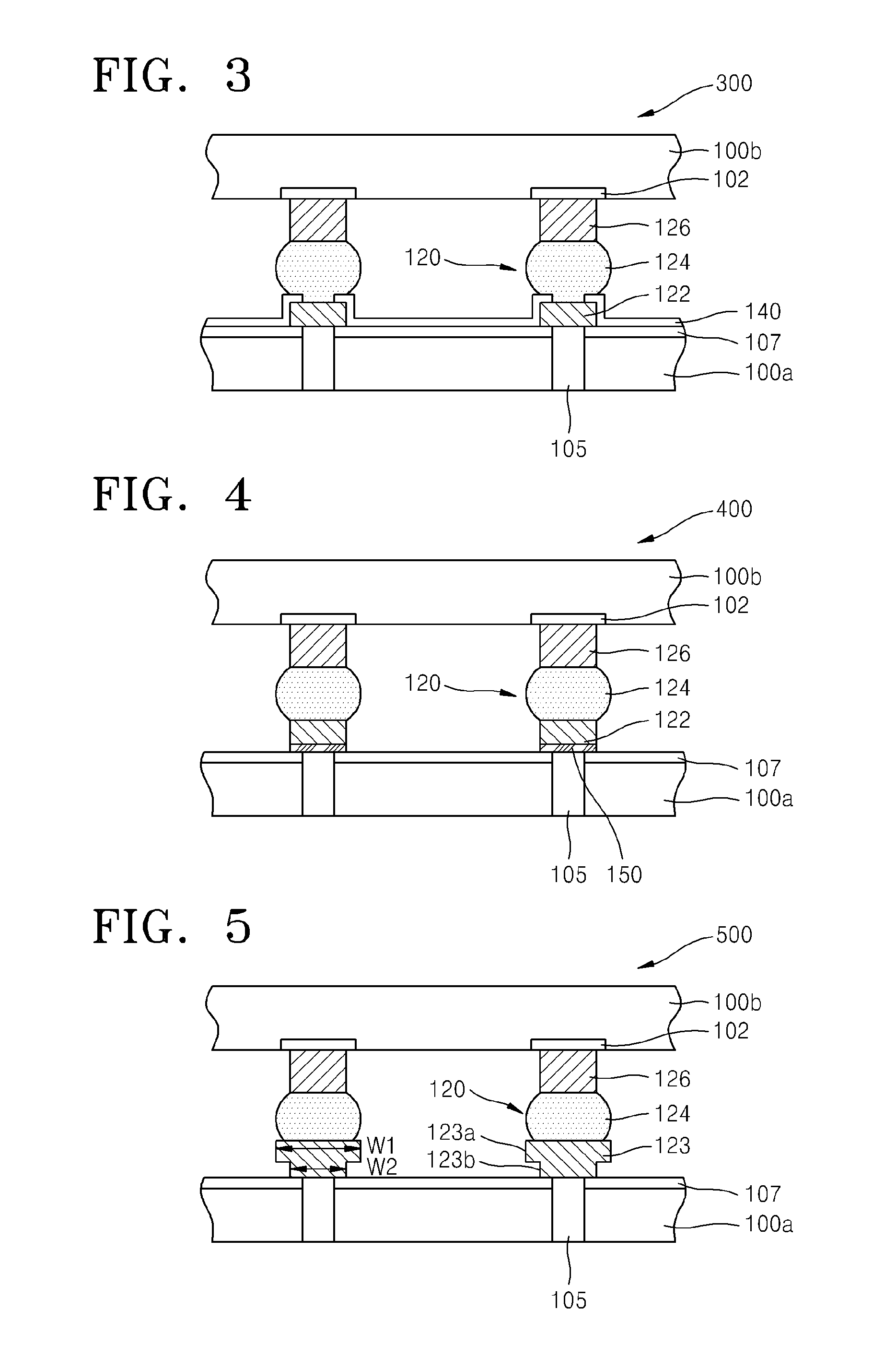
[0031]Reference will now be made in detail to the exemplary embodiments of the present general inventive concept, examples of which are illustrated in the accompanying drawings, wherein like reference numerals refer to the like elements throughout. The exemplary embodiments are described below in order to explain the present general inventive concept while referring to the figures.

[0032]Embodiments of the present general inventive concept are described herein with reference to cross-section illustrations that are schematic illustrations of exemplary embodiments (and intermediate structures) of the present general inventive concept. As such, variations from the shapes of the illustrations as a result, for example, of manufacturing techniques and / or tolerances, are to be expected. Thus, embodiments of the present general inventive concept should not be construed as limited to the particular shapes of regions illustrated herein but are to include deviations in shapes that result, for e...


PUM


Abstract

A semiconductor package includes a first semiconductor chip, a second semiconductor chip disposed on the first semiconductor chip, and a connection member to electrically connect the first semiconductor chip and the second semiconductor chip. The connection member may include a connection pad disposed on the first semiconductor chip, a connection pillar disposed on the second semiconductor chip, and a bonding member to connect the connection pad and the connection pillar. An anti-contact layer may be formed on at least one surface of the connection pad.

Description

CROSS-REFERENCE TO RELATED APPLICATIONS[0001]This application claims priority under 35 U.S.C. §119(a) from Korean Patent Application No. 10-2011-0103047, filed on Oct. 10, 2011, in the Korean Intellectual Property Office, the disclosure of which is incorporated herein in its entirety by reference.BACKGROUND[0002]1. Field[0003]The general inventive concept relates to semiconductor packages, and more particularly, to a semiconductor package including connection members to connect semiconductor chips.[0004]2. Description of the Related Art[0005]As electronic products are tending to become thinner, smaller and lighter, semiconductor devices and semiconductor packages are also becoming thinner, smaller and lighter. A process of miniaturizing a semiconductor device is accompanied by limitations to increase the performance of a semiconductor chip, e.g., a signal delay, caused by an increase in interconnection lines. To solve this problem, a technique of stacking a plurality of semiconducto...

Claims


Application Information

Patent Timeline
IPC IPC(8): H01L23/498H01L23/48
CPCH01L25/0657H01L2224/16145H01L2225/06517H01L2924/1431H01L2924/1432H01L2924/1433H01L2924/1434H01L2924/1436H01L2924/1437H01L2924/1438H01L2924/1443H01L2924/15311H01L2225/06513H01L2225/06541H01L2225/06565H01L2224/03614H01L24/03H01L24/05H01L24/13H01L24/16H01L2224/0345H01L2224/03452H01L2224/03462H01L2224/0347H01L2224/0361H01L2224/0401H01L2224/05025H01L2224/05082H01L2224/05124H01L2224/05147H01L2224/05166H01L2224/05557H01L2224/05562H01L2224/05611H01L2224/05647H01L2224/05655H01L2224/05687H01L2224/06181H01L2224/13082H01L2224/13111H01L2224/13147H01L2224/13155H01L2224/16148H01L2224/16237H01L2224/81191H01L2224/81385H01L2224/81395H01L2224/8181H01L2224/81815H01L2224/05568H01L2224/03622H01L2224/05023H01L2224/16503H01L2224/05565H01L2924/01029H01L2224/10145H01L2224/05547H01L2224/05686H01L2224/02175H01L2924/01327H01L2924/00014H01L2924/05042H01L2924/00H01L2224/05552H01L2924/15787H01L2224/13023H01L2224/05007H01L23/48H01L23/488
Inventor JEE, YOUNG-KUNSEO, SUN-KYOUNGPARK, SANG-WOOKHWANG, JI-HWAN
Owner SAMSUNG ELECTRONICS CO LTD
Why Eureka
Try Eureka