Method of Fabricating a Substrate Having Conductive Through Holes

a technology of through holes and substrates, which is applied in the manufacture of printed circuits, electrical devices, printed circuits, etc., can solve the problems of misalignment of metal masks, complex overall process, and difficulty in completely filling through holes

Inactive Publication Date: 2013-04-11
VIKING TECH L C
View PDF0 Cites 4 Cited by
  • Summary
  • Abstract
  • Description
  • Claims
  • Application Information

AI Technical Summary

Benefits of technology

[0016]In conclusion, the method of fabricating the substrate having the conductive through holes of this invention is free from the misalignment problem of the prior art by self-deposition of metal in the through holes. In addition, the conductive through holes and a surface circuit layer of this invention are fabricated separately such that the thickness of the circuit layer can be fabricated according to requirements of clients without being limited by the fabricating process of the conductive through holes.

Problems solved by technology

However, the metal masks 11 are subject to a misalignment problem, especially at the edges of the substrate 10, where misalignment accumulates.
The overall process is complicated and it is not easy to completely fill up the through holes.
And it leads to the copper layer formed on the surface of the substrate becoming too thick such that the overall thickness of the substrate exceeds the required specification of clients.
Moreover, dimples are readily formed on the surface of the substrate at the through holes due to the inherent problem of electroplating filling.
Besides, the longer time of overall process also affects the yield and cost of substrates.

Method used


Image

  • Method of Fabricating a Substrate Having Conductive Through Holes
  • Method of Fabricating a Substrate Having Conductive Through Holes
  • Method of Fabricating a Substrate Having Conductive Through Holes

Examples


Embodiment Construction

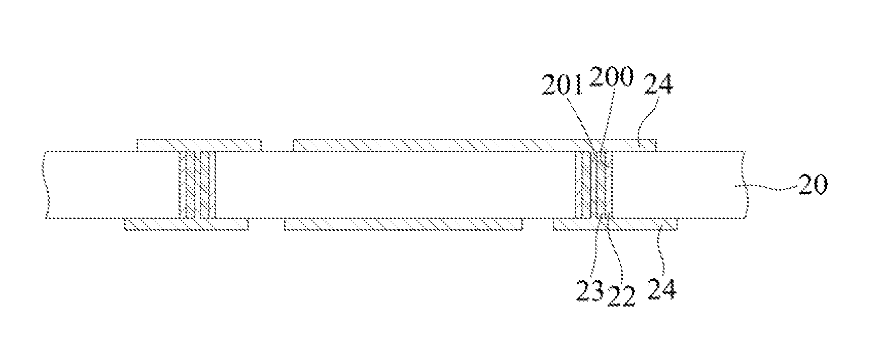
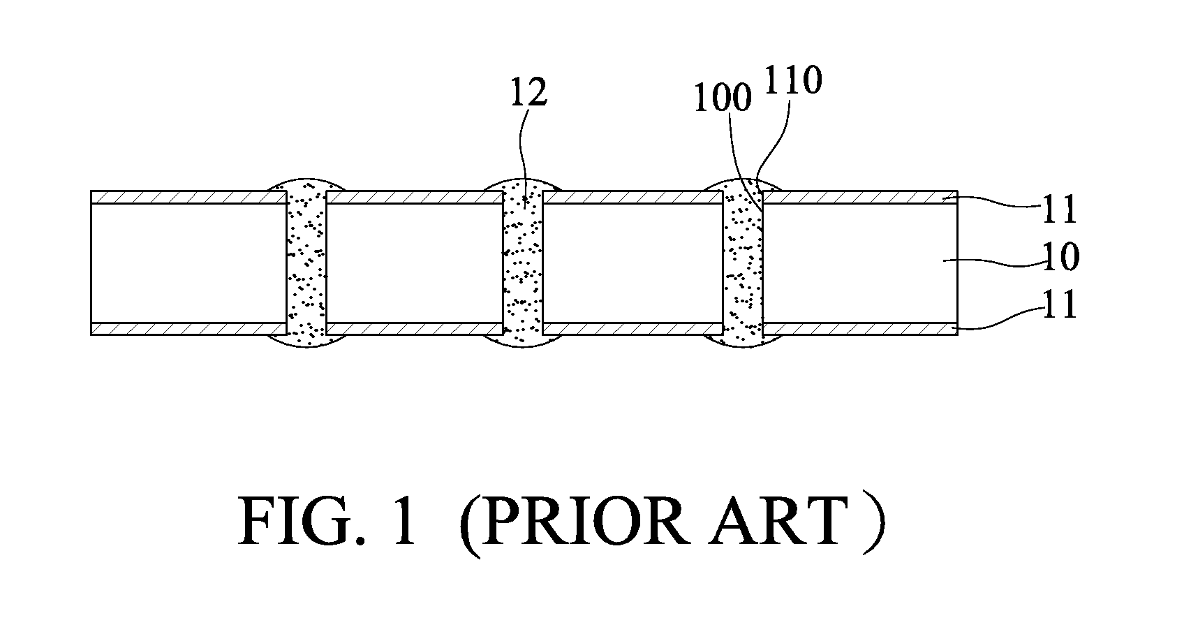
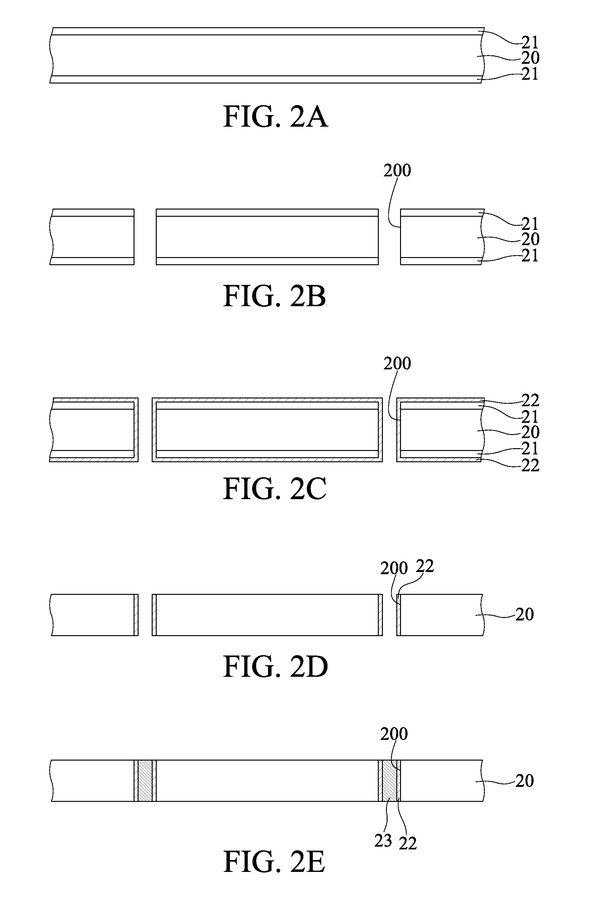
[0019]The following illustrative embodiments are provided to illustrate the disclosures of this invention, these and other advantages and effects can be apparently understood by those in the art after reading the disclosures of this specification.

[0020]Note that the structures, proportions, sizes depicted in the accompanying figures merely illustrate the disclosures of the specification to allow for comprehensive reading without a limitation to the implementation or applications of this invention, and does not constitute any substantial technical meaning. Any variations or alterations to the structures, proportional relations or sizes should be encompassed within the scope of the disclosures without affecting effects generated by and objectives achieved by this invention. Meanwhile, the terms that are quoted in the explanation like “upper,”“side,”“a” and so on only intent for convenience of description rather than limiting feasible scope of the disclosed embodiments. Change or adjus...


PUM

PropertyMeasurementUnit
conductiveaaaaaaaaaa
electricallyaaaaaaaaaa
areaaaaaaaaaaa

Abstract

A method of fabricating a substrate having a plurality of conductive through holes is disclosed. Release films are formed on opposite sides of a substrate, and a plurality of through holes penetrating the release films and the substrate are formed. A first metal layer is formed on the release films and the sidewall of each of the through holes prior to removing the release films and the first metal layer thereon. A second metal layer is formed on the first metal layer on the sidewalls of the through holes by electroless plating. Compared to the prior art, the method is simpler and cheaper to carry out while the conductive through holes and a surface circuit layer thereof are fabricated separately, thereby avoiding disadvantage of forming a circuit layer on the surface of the substrate too thick.

Description

BACKGROUND OF THE INVENTION[0001]1. Field of the Invention[0002]This invention relates to methods of fabricating a substrate, and, more particularly, to a method of fabricating a substrate having conductive through holes.[0003]2. Description of Related Art[0004]In order to take the full advantage of the substrate area and reduce the transmission route of electronic signals, the substrate has through holes penetrating therethrough and filled with conductive material so as to form conductive through holes for circuits and electronic elements disposed on the substrate to be electrically connected thereto.[0005]Referring to FIG. 1, a cross-sectional diagram of a substrate having conductive through holes in accordance with the prior art is provided. A plurality of through holes 100 are formed to penetrate a substrate 10, and metal masks 11 are disposed on both surfaces of the substrate 10. Each of the metal masks 11 has a plurality of openings 110 corresponding in position to the through...

Claims


Application Information

Patent Timeline
Patent Type & Authority Applications(United States)
IPC IPC(8): H01L21/768
CPCH05K3/426H05K1/0306
Inventor WEI, SHIH-LONGHSIAO, SHEN-LIHO, CHIEN-HUNG
Owner VIKING TECH L C
Why Eureka
Try Eureka