Ceramic substrate and method of manufacturing the same

a ceramic substrate and substrate technology, applied in the direction of conductive pattern formation, synthetic resin layered products, chemistry apparatus and processes, etc., can solve the problems of high positional accuracy of the substrate body, difficult to accurately form the conductor layer at each predetermined position, and difficult to accurately form the conductor layer at the same position in plan view. achieve the effect of reducing misalignment between the first and second conductor layers and high positional accuracy

Active Publication Date: 2013-05-09
NGK SPARK PLUG CO LTD
View PDF6 Cites 0 Cited by
  • Summary
  • Abstract
  • Description
  • Claims
  • Application Information

AI Technical Summary

Benefits of technology

[0008]The invention has been made to solve the problem described in the background art, and an object of the invention is to provide a ceramic substrate that has a small misalignment between conductor layers formed on the surface and the back of a substrate body made of ceramic, that is, a small misalignment between patterns of conductor layers formed on the surface and back, and a method of reliably manufacturing the substrate.

Problems solved by technology

However, according to the method of manufacturing the ceramic wiring substrate, it is possible to accurately set the print positions of the wiring patterns between the plurality of green sheets but it is very difficult to accurately form a conductor layer at each predetermined position in plan view on both the surface and the back of the substrate body where a plurality of ceramic layers are laminated.
For example, in the above-mentioned method, it is very difficult to form conductor layers at the same positions in plan view on both the surface and the back of the substrate body with high positional accuracy.

Method used


Image

  • Ceramic substrate and method of manufacturing the same
  • Ceramic substrate and method of manufacturing the same
  • Ceramic substrate and method of manufacturing the same

Examples


Embodiment Construction

[0077]Embodiments of the invention will be described below.

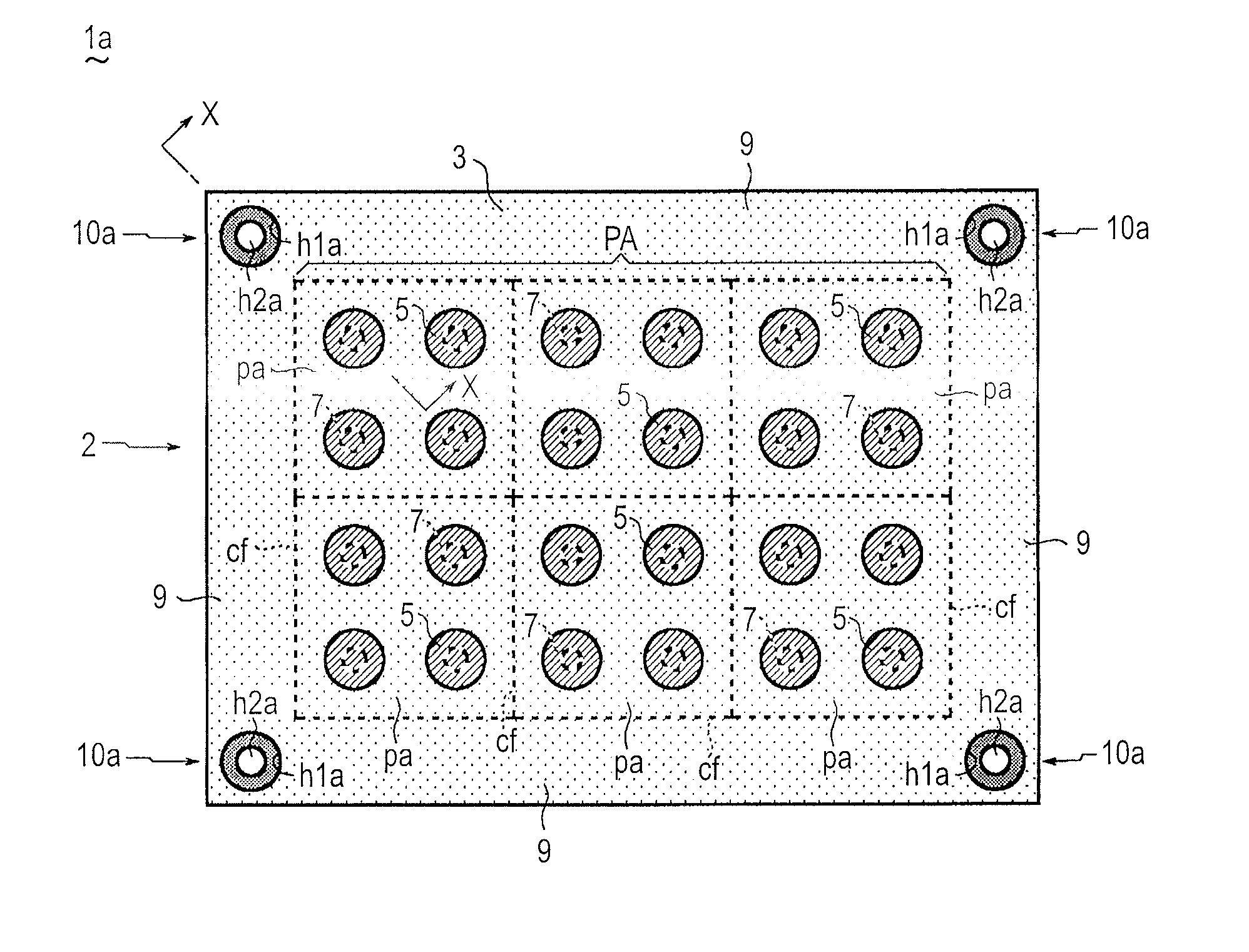
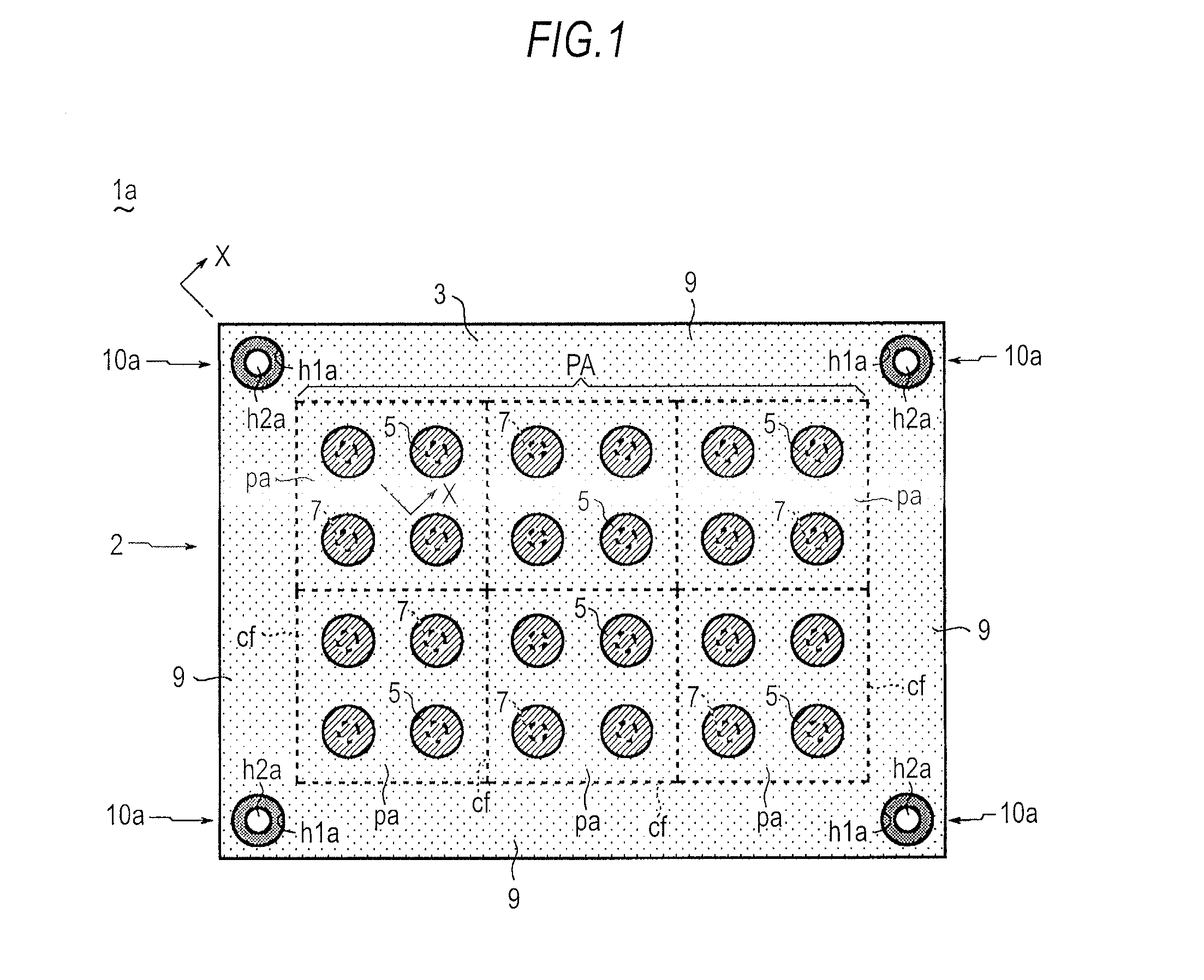
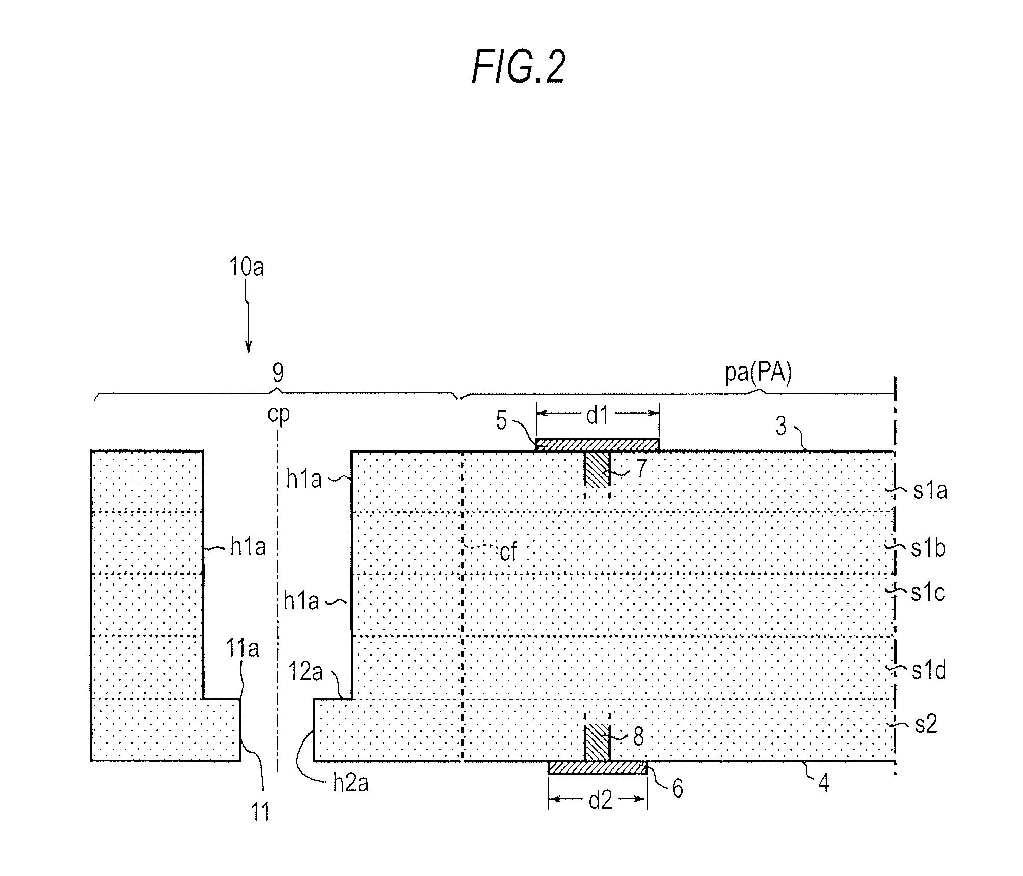
[0078]FIG. 1 is a plan view of a first ceramic substrate 1a according to the invention, and FIG. 2 is a vertical cross-sectional view where a portion taken along line X-X of FIG. 1 is enlarged.

[0079]The first ceramic substrate 1a is a multi-piece substrate. As shown in FIGS. 1 and 2, the first ceramic substrate 1a includes a substrate body 2, first conductor layers (pads) 5 that are formed on the surface (one principal surface) 3 of the substrate body 2, second conductor layers 6 which are formed on the back (the other principal surface) 4 of the substrate body 2 and each of which has a diameter d2 smaller than a diameter d1 of each first conductor layer 5 in plan view, via conductors (conductor posts) 7 and 8 that are individually connected to the first and second conductor layers 5 and 6 and formed in the substrate body 2, and a plurality of (four) positioning portions 10a each of which is formed at each corner portion of ...


PUM

PropertyMeasurementUnit
diameteraaaaaaaaaa
lengthaaaaaaaaaa
thicknessaaaaaaaaaa

Abstract

A ceramic substrate includes: a substrate body formed by laminating a plurality of ceramic layers and including a first and second opposing principal surfaces and a peripheral portion having a positioning portion; a first conductor pad formed on the first principal surface; a second conductor pad formed on the second principal surface and having a diameter smaller than that of the first conductor pad. The positioning portion includes first and second through holes that individually pass through respective ceramic layers and are connected to each other in an axial direction. The first through hole passes through the first principal surface. The second through hole passes through the second principal surface and has a cross-sectional area that is smaller than that of the first through hole. At least apart of a peripheral edge of a ceramic layer defining the second through hole is visible through the first through hole.

Description

CROSS REFERENCE TO RELATED APPLICATIONS[0001]The present application claims priority from Japanese Patent Application No. 2011-244427, which was filed on Nov. 8, 2011, the disclosure of which is herein incorporated by reference in its entirety.BACKGROUND OF THE INVENTION[0002]1. Field of the Invention[0003]The present invention relates to a ceramic substrate that has a small relative misalignment between conductor layers formed on the surface and the back of a substrate body made of ceramic and includes the conductor layers formed with high positional accuracy, and a method of manufacturing the ceramic substrate.[0004]2. Description of Related Art[0005]To reduce a misalignment between layers of a plurality of ceramic green sheets and to suppress the deterioration of electrical characteristics caused by the misalignment of wiring patterns between the layers, there is proposed a method of manufacturing a ceramic multilayer wiring board. The method includes a first process for forming ...

Claims


Application Information

Patent Timeline
Patent Type & Authority Applications(United States)
IPC IPC(8): H05K1/03H05K3/10H05K1/11
CPCH05K3/4629H05K2201/09063H05K3/4638
Inventor SUZUKI, KENJIOTSUKA, YUMANASU, TAKAKUNI
Owner NGK SPARK PLUG CO LTD
Why Eureka
Try Eureka