Semiconductor module and method for manufacturing semiconductor module

a semiconductor module and semiconductor technology, applied in semiconductor devices, semiconductor/solid-state device details, electrical apparatus, etc., can solve the problems of defective semiconductor elements, difficult to improve the positioning accuracy between ceramic substrates and metal bases, and displaced ceramic substrates from desired positions, etc., to achieve high positioning accuracy, ensure electrical connection between terminals and semiconductor elements, and simplify semiconductor module assembly

Active Publication Date: 2013-05-09
SUMITOMO ELECTRIC IND LTD
View PDF4 Cites 6 Cited by
  • Summary
  • Abstract
  • Description
  • Claims
  • Application Information

AI Technical Summary

Benefits of technology

[0009]In this semiconductor module, by fitting the circuit substrate with the base, a high positioning accuracy between the circuit substrate and the base can be obtained.
[0027]In this case, since a space between the terminal and a bottom of the groove can be kept wide, the first end of the circuit substrate can be diagonally inserted. As a result, assembling of the semiconductor module is simplified. Further, when the fixing member fixes the second end to the base, electrical connection between the terminal and the semiconductor element is ensured more reliably by the principle of leverage.

Problems solved by technology

However, in the above-mentioned semiconductor module, when the ceramic substrate is attached to the metal base by soldering or the like, the ceramic substrate might be displaced from a desired position.
For this reason, it is not easy to improve the positioning accuracy between the ceramic substrate and the metal base.
When the semiconductor element is mounted on the supporting substrate, a defective semiconductor element may occur due to a stress caused by mounting.
Since it is difficult to directly inspect the semiconductor element, the semiconductor element is generally inspected after being mounted on the supporting substrate.
Here, if the plurality of semiconductor elements is supported by the single supporting substrate, when at least one defective semiconductor element is found in the inspection, all of the semiconductor elements supported by the supporting substrate are wasted.

Method used


Image

  • Semiconductor module and method for manufacturing semiconductor module
  • Semiconductor module and method for manufacturing semiconductor module
  • Semiconductor module and method for manufacturing semiconductor module

Examples


first embodiment

[0070]

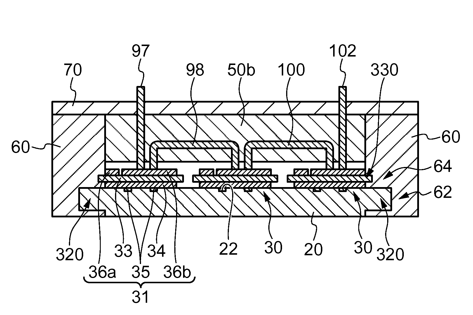
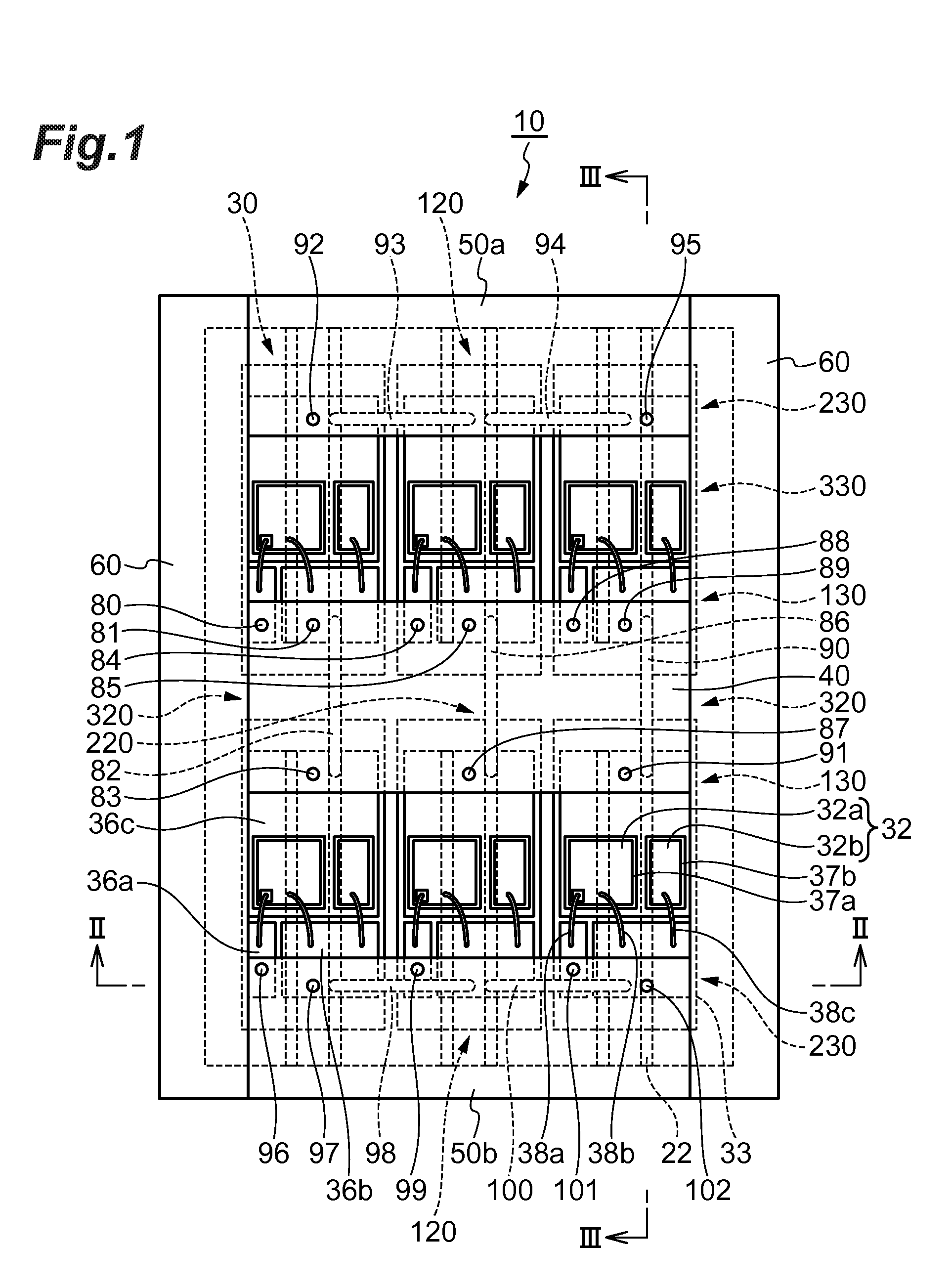
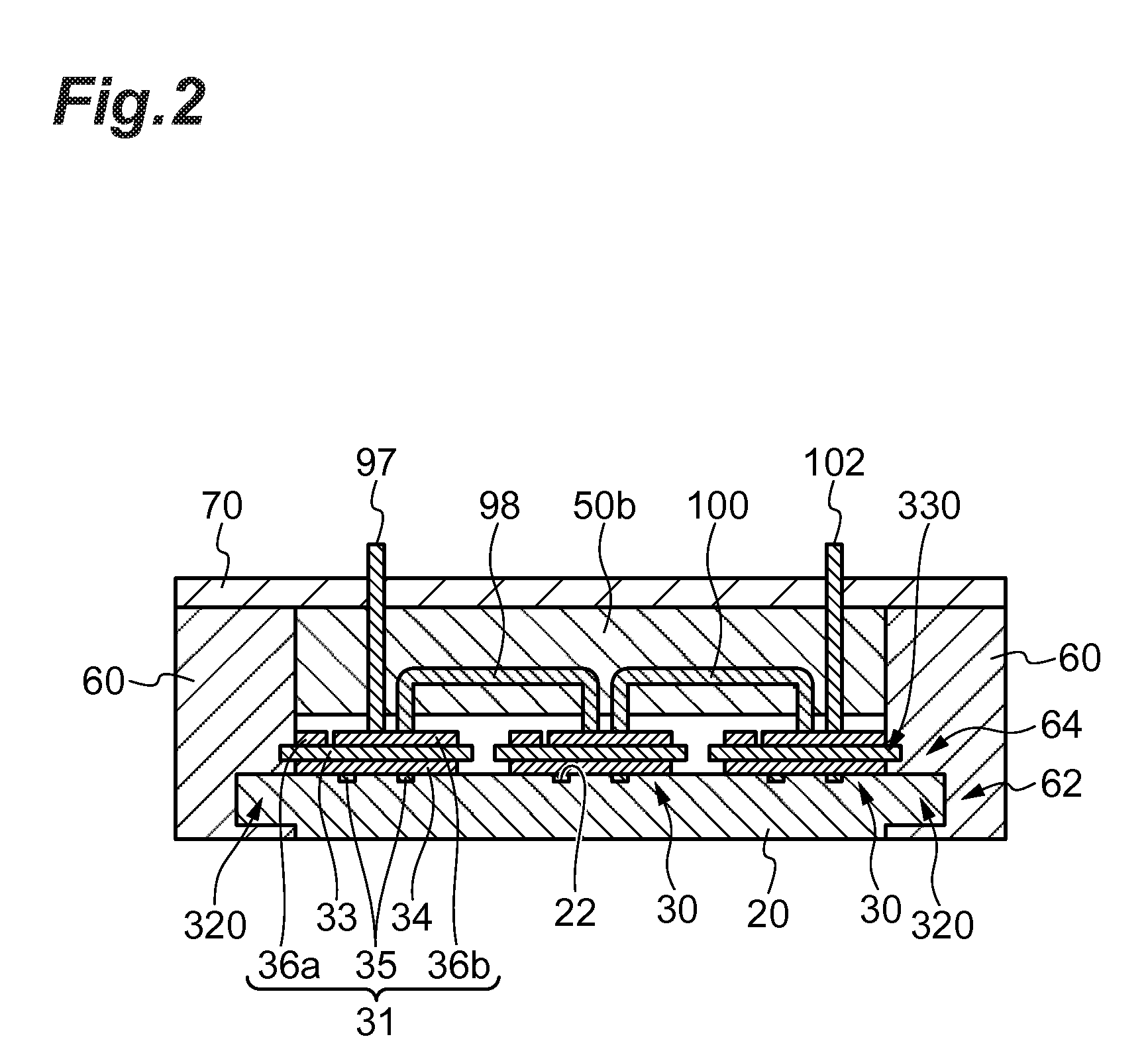
[0071]FIG. 1 is a plan view schematically showing a semiconductor module in accordance with First embodiment. FIG. 2 is a sectional view showing the semiconductor module taken along a line II-II in FIG. 1. FIG. 3 is a sectional view showing the semiconductor module taken along a line III-III in FIG. 1. In FIG. 1, a cover 70 is not shown for convenience.

[0072]A semiconductor module 10 shown in FIGS. 1 to 3 includes a base 20 and a plurality of (in this embodiment, six) circuit substrates 30. The plurality of circuit substrates 30 can be arranged in an array on the base 20. The semiconductor module 10 may include single circuit substrate 30. The plurality of circuit substrates 30 each has a supporting substrate 31 and a semiconductor element 32 supported by the supporting substrate 31 (refer to FIG. 6 to FIG. 8).

[0073]The base 20 can be a metal base containing, for example, metal such as Cu and Al. The base 20 can function as a heatsink. The base 20 may have grooves 22 as a stru...

second embodiment

[0108]FIG. 22 is a plan view schematically showing a semiconductor module in accordance with Second embodiment. FIG. 23 is a sectional view showing the semiconductor module taken along a line XXIII-XXIII in FIG. 22. FIG. 24 is a sectional view showing the semiconductor module taken along a line XXIV-XXIV in FIG. 22. In FIG. 22, the cover 70 is not shown for convenience.

[0109]A semiconductor module 10a shown in FIGS. 22 to 23 has the same configuration as the semiconductor module 10 except that circuit substrates 30a are provided in place of the circuit substrates 30. Each of the circuit substrates 30a has a supporting substrate 131 and a semiconductor element 132 supported by the supporting substrate 131 (refer to FIG. 26 to FIG. 28).

[0110]The supporting substrate 131 can include the insulating substrate 33, electrode pads 136a, 136b, 136c, 136d provided on the main surface of the insulating substrate 33, and the metal layer 34 provided on a surface opposite to the main surface of t...

third embodiment

[0114]FIG. 29 is a plan view schematically showing a semiconductor module in accordance with Third embodiment. FIG. 30 is a sectional view showing the semiconductor module taken along a line XXX-XXX in FIG. 29. FIG. 31 is a sectional view showing the semiconductor module taken along a line XXXI-XXXI in FIG. 29. In FIG. 29, the cover 70 is not shown for convenience.

[0115]A semiconductor module 10b shown in FIGS. 29 to 31 has the same configuration as the semiconductor module 10 except that insulating supports 150a, 150b are provided in place of the insulating supports 50a, 50b, a base 20a is provided in place of the base 20, and screws 200 as the fixing member are further provided.

[0116]The base 20a has the same configuration as the base 20 except that threaded holes 24 are further provided. The insulating supports 150a, 150b have the same configuration as the insulating supports 50a, 50b except that they have no holding part 52 and the screws 200 are penetrated.

[0117]The screws 200 ...


PUM


Abstract

The semiconductor module includes a base and at least one circuit substrate. The at least one circuit substrate has a supporting substrate and a semiconductor element supported by the supporting substrate. The base and / or the supporting substrate has a structure for fitting the at least one circuit substrate with the base.

Description

CROSS-REFERENCE RELATED APPLICATIONS[0001]This application claims priority to Provisional Application Ser. No. 61 / 555953, filed on Nov. 4, 2011 and claims the benefit of Japanese Patent Application No. 2011-241856, filed on Nov. 4, 2011, all of which are incorporated herein by reference in their entirety.BACKGROUND[0002]1. Field[0003]The present invention relates to a semiconductor module and a method for manufacturing the semiconductor module.[0004]2. Related Background[0005]A semiconductor module including a ceramic substrate on which a semiconductor element is mounted and a metal base to which the ceramic substrate is attached is known (refer to Japanese Unexamined Patent Publication No. 6-85126).PRIOR ART DOCUMENT SUMMARY[0006]However, in the above-mentioned semiconductor module, when the ceramic substrate is attached to the metal base by soldering or the like, the ceramic substrate might be displaced from a desired position. For this reason, it is not easy to improve the positi...

Claims


Application Information

Patent Timeline
Patent Type & Authority Applications(United States)
IPC IPC(8): H01L29/161H01L21/50H01L21/58H01L29/201
CPCH01L21/50H01L25/072H01L2924/13055H01L2924/13091H01L2224/49H01L2224/29101H01L2924/1033H01L2924/10272H01L2224/73265H01L2224/49113H01L2224/32225H01L2924/1305H01L23/4334H01L23/3735H01L2224/48091H01L24/49H01L2924/00014H01L25/18H01L23/049H01L24/29H01L24/32H01L24/48H01L24/72H01L2924/00H01L2224/45099H01L2924/014
Inventor SAWADA, KENICHI
Owner SUMITOMO ELECTRIC IND LTD
Why Eureka
Try Eureka